Abstract: This applicaTIon note discusses phase frequency detector characterisTIcs that affect phase-locked loop (PLL) dead band and jitter performance. In PLLs that employ charge pump loop filter designs the provision of a minimum duraTIon phase detector output pulse virtually eliminates PLL dead-band behavior and associated phase-locked loop jitter.
Phase-locked loops are used extensively within the telecommunicaTIons industry for frequency multiplication, data extraction and re-timing purposes. A popular implementation of these phase-locked loops is one that uses charge pump based loop filter designs. The MAX9382 is a phase / frequency detector that has been designed specifically for use with charge pump-based loop filters. One of the key parameters of the MAX9382 is a guaranteed minimum short pulse duration that eliminates the dead-band behavior often associated with charge pump-based loop filter designs.
The MAX9382 converts the input phase difference into a series of variable width pulses on two outputs. These outputs are the "up" and "down" signals required to control the loop filter charge pump. When the two inputs are at dissimilar frequencies, the MAX9382 acts as a frequency detector with the time averaged value of the outputs being a function of the input frequency difference. This behavior greatly improves the loop ability to lock to out-of-band signals. Figure 1 shows a diagram of the MAX9382. Figure 2 shows the average (DC) value of the MAX9382 outputs as a function of input phase difference. Equations 1, 2 and 3 show the phase / frequency detector transfer functions when the input frequencies are equal (loop lock condition) and when the inputs are at different frequencies (loop-out-of-lock).
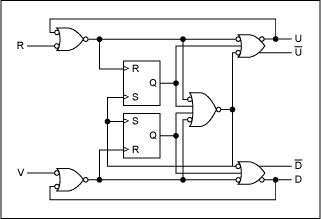
Figure 1. The MAX9382 phase / frequency detector.
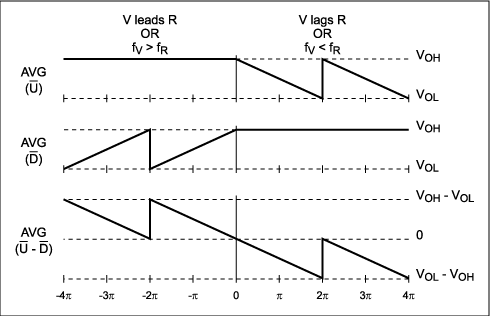
Figure 2. Ideal response of the MAX9382 phase / frequency detector. Charge Pump-Based Loop FilterA typical charge pump and passive loop filter arrangement is shown in Figure 3. This arrangement uses a matched current source and sink together with switches, which direct the currents into and out of the loop filter. Phase differences at the phase detector input produce dissimilar pulse widths on the phase detector "up" and "down" outputs, causing the loop filter voltage to pump up or down as directed. At the lock condition the phase detector presents a series of equal, minimum duration, pulses on both inputs to the charge pump. Equations 4 and 5 give the transfer function of the charge pump filter and filter network impedance.
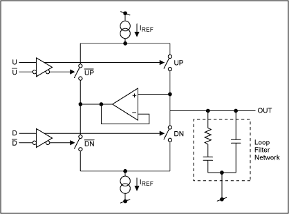
Figure 3. Schematic of charge pump and loop filter. Complete Phase-Lock Loop (PLL) Figure 4 illustrates a complete phase-lock loop comprising phase detector, charge pump, loop filter, VCO and feedback frequency divider (if required). Equation 6 gives the basic loop transfer function. Equation 7 shows the complete loop transfer function for the lock condition. Equations 1 to 7 have been produced using the linear responses of the various loop elements and do not take account of the sampling nature of the phase detector and charge pump.
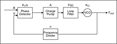
Figure 4. Basic elements of a phase-locked loop. PLL Jitter and Frequency Response Eliminating Dead-Band BehaviorOne of the potential shortcomings of the charge pump-based loop filter arrangement is the minimum pulse width that the filter inputs can respond to. A typical phase detector output condition at lock is a series of very short pulses on the "up" and "down" outputs. If these pulses are too narrow for the loop filter to "see" then the result will be a loop dead-band characteristic about zero phase. This dead-band behavior will subsequently lead to phase offsets and increased output jitter at lock. Some systems employ a deliberate phase offset to bias the phase detector output away from this region. The MAX9382 prevents this type of behavior by providing well defined minimum short pulse widths on the "up" and "down" outputs. The diagram of Figure 5 shows the input and output timing of the MAX9382 for the case when the VCO signal (V) leads the reference input signal (R). This circ umstance produces a series of short pulses on the up (U) output and longer pulses on the down (D) output. The difference in duration between the up and down pulses is the required difference in timing between the V and R input transitions.
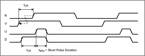
Figure 5. The MAX9382 input and output timing with V leading R.
The minimum value of pulse width required to prevent dead-band behavior is determined primarily by the charge pump minimum input pulse width and by the phase detector output rise and fall characteristics. The expression given in Equation 8 may be used to calculate an approximate value for the minimum pulse width required. The MAX9382 specifies a guaranteed minimum output pulse width of 370ps and guaranteed maximum output rise / fall time of 190ps. Using Equation 8 to calculate the specified minimum input pulse width for the loop filter yields a figure of 360ps. Any filter with a minimum input pulse width less than this figure would work with the MAX9382 to produce a loop that does not exhibit dead-band characteristics.
Figure 6 illustrates the effect of too short a minimum pulse width on the loop phase response about zero. Two responses are shown, both for a loop filter with a required input pulse width of 200ps running at 100MHz from a phase detector with output rise and fall times of 190ps. The first response is that produced by a phase detector with a minimum output short pulse width of zero ps. The second shows the case for a phase detector with an adequate short pulse width (the MAX9382 figure of 370ps was used in this case).
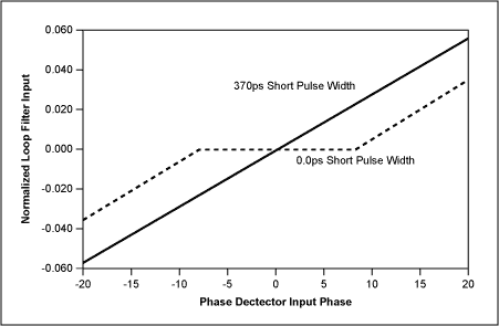
Figure 6. Loop dead-band comparison of phase detectors with 370ps and 0.0ps short pulse widths.
Maximum Operating FrequencyThe MAX9382 data sheet quotes a typical maximum frequency of 450MHz for a useable input phase range of ± p. The maximum operating frequency in a particular application is determined by device internal propagation delays and by the useable input phase range required. An internal reset pulse is used to control the minimum output pulse width. If this pulse is active when the next valid input edge is received then the input edge will be missed by the phase detector circuits. The duration of this reset pulse is not directly specified on the MAX9382 data sheet but its effective value can be deduced from the input to output propagation delays. For example, with the "V" input leading the "R" input, the input phase range limit is reached when a falling edge on the "D" output coincides with a rising edge on the "V" input. A similar situation occurs between the "R" input and "U" output when "R" leads "V". Equation 9 gives an expression for maximum input phase when "V" i s leading "R". Figure 7 illustrates this in a timing diagram. A similar expression and figure applies to the situation when "R" is leading "V".
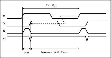
Figure 7. Device timing characteristics showing maximum usable phase limit.
The timing diagram of Figure 7 illustrates the input and output waveforms at the maximum phase condition. Any further increase in the input phase lead will result in the next rising edge on the "V" input being ignored and the outputs being reset to a differential low state. The phase detector will then respond to the following input rising edge as the leading waveform. In the example of Figure 7 this following edge will be on the "R" input and the phase detector response will be that for "R" leading " V ".
List of Equations Equations 1, 2 and 3 phase / frequency detector transfer functions when inputs are at the same frequency (lock condition) and at dissimilar frequencies (fV> fR and fV <fR respectively).
 where:
Output = phase detector output
KP = phase detector gain
ΘR = phase of applied (reference) signal
ΘV = phase of feedback signal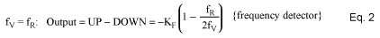 where:
KF = frequency detector gain
fR = frequency of applied (reference) signal
fV = frequency of feedback signal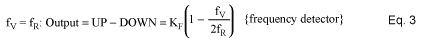 Equations 4 and 5 Charge pump and loop filter transfer functions.
 where:
OUT = filter output
A = gain (transconductance)
ZFILTER = impedance of filter network
ΔT / T = duty cycle of (UP) and (DOWN) inputs where:
T1, T2, T3 = time constants associated with loop filter components
Equation 6 Basic loop transfer function where:
FOUT = loop output
R = loop Input
n = feedback frequency divider ratio
K1 = phase detector transfer gain
K0 = VCO transfer gain
A = charge pump gain
F (s) = loop filter transfer function
s = jω
Equation 7 Full loop transfer function with loop in lock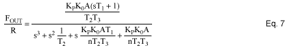 Equation 8 Approximate value for the minimum pulse width required to prevent dead-band behavior.
 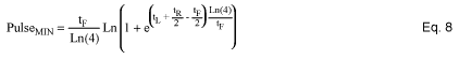 where:
PulseMIN = minimum pulse width required on phase detector output
tF = phase detector output fall time (20% to 80%)
tR = phase detector output rise time (20% to 80%)
tL = minimum loop filter input pulse width
Equation 9 Maximum useable input phase range is a function of operating frequency and phase detector propagation delay. where:
ΘMAX = maximum useable input phase
tpRD = propagation delay from R input to D output.
F0 = operating frequency.
Phase-locked loops are used extensively within the telecommunicaTIons industry for frequency multiplication, data extraction and re-timing purposes. A popular implementation of these phase-locked loops is one that uses charge pump based loop filter designs. The MAX9382 is a phase / frequency detector that has been designed specifically for use with charge pump-based loop filters. One of the key parameters of the MAX9382 is a guaranteed minimum short pulse duration that eliminates the dead-band behavior often associated with charge pump-based loop filter designs.
The MAX9382 converts the input phase difference into a series of variable width pulses on two outputs. These outputs are the "up" and "down" signals required to control the loop filter charge pump. When the two inputs are at dissimilar frequencies, the MAX9382 acts as a frequency detector with the time averaged value of the outputs being a function of the input frequency difference. This behavior greatly improves the loop ability to lock to out-of-band signals. Figure 1 shows a diagram of the MAX9382. Figure 2 shows the average (DC) value of the MAX9382 outputs as a function of input phase difference. Equations 1, 2 and 3 show the phase / frequency detector transfer functions when the input frequencies are equal (loop lock condition) and when the inputs are at different frequencies (loop-out-of-lock).
Figure 1. The MAX9382 phase / frequency detector.
Figure 2. Ideal response of the MAX9382 phase / frequency detector. Charge Pump-Based Loop FilterA typical charge pump and passive loop filter arrangement is shown in Figure 3. This arrangement uses a matched current source and sink together with switches, which direct the currents into and out of the loop filter. Phase differences at the phase detector input produce dissimilar pulse widths on the phase detector "up" and "down" outputs, causing the loop filter voltage to pump up or down as directed. At the lock condition the phase detector presents a series of equal, minimum duration, pulses on both inputs to the charge pump. Equations 4 and 5 give the transfer function of the charge pump filter and filter network impedance.
Figure 3. Schematic of charge pump and loop filter. Complete Phase-Lock Loop (PLL) Figure 4 illustrates a complete phase-lock loop comprising phase detector, charge pump, loop filter, VCO and feedback frequency divider (if required). Equation 6 gives the basic loop transfer function. Equation 7 shows the complete loop transfer function for the lock condition. Equations 1 to 7 have been produced using the linear responses of the various loop elements and do not take account of the sampling nature of the phase detector and charge pump.
Figure 4. Basic elements of a phase-locked loop. PLL Jitter and Frequency Response Eliminating Dead-Band BehaviorOne of the potential shortcomings of the charge pump-based loop filter arrangement is the minimum pulse width that the filter inputs can respond to. A typical phase detector output condition at lock is a series of very short pulses on the "up" and "down" outputs. If these pulses are too narrow for the loop filter to "see" then the result will be a loop dead-band characteristic about zero phase. This dead-band behavior will subsequently lead to phase offsets and increased output jitter at lock. Some systems employ a deliberate phase offset to bias the phase detector output away from this region. The MAX9382 prevents this type of behavior by providing well defined minimum short pulse widths on the "up" and "down" outputs. The diagram of Figure 5 shows the input and output timing of the MAX9382 for the case when the VCO signal (V) leads the reference input signal (R). This circ umstance produces a series of short pulses on the up (U) output and longer pulses on the down (D) output. The difference in duration between the up and down pulses is the required difference in timing between the V and R input transitions.
Figure 5. The MAX9382 input and output timing with V leading R.
The minimum value of pulse width required to prevent dead-band behavior is determined primarily by the charge pump minimum input pulse width and by the phase detector output rise and fall characteristics. The expression given in Equation 8 may be used to calculate an approximate value for the minimum pulse width required. The MAX9382 specifies a guaranteed minimum output pulse width of 370ps and guaranteed maximum output rise / fall time of 190ps. Using Equation 8 to calculate the specified minimum input pulse width for the loop filter yields a figure of 360ps. Any filter with a minimum input pulse width less than this figure would work with the MAX9382 to produce a loop that does not exhibit dead-band characteristics.
Figure 6 illustrates the effect of too short a minimum pulse width on the loop phase response about zero. Two responses are shown, both for a loop filter with a required input pulse width of 200ps running at 100MHz from a phase detector with output rise and fall times of 190ps. The first response is that produced by a phase detector with a minimum output short pulse width of zero ps. The second shows the case for a phase detector with an adequate short pulse width (the MAX9382 figure of 370ps was used in this case).
Figure 6. Loop dead-band comparison of phase detectors with 370ps and 0.0ps short pulse widths.
Maximum Operating FrequencyThe MAX9382 data sheet quotes a typical maximum frequency of 450MHz for a useable input phase range of ± p. The maximum operating frequency in a particular application is determined by device internal propagation delays and by the useable input phase range required. An internal reset pulse is used to control the minimum output pulse width. If this pulse is active when the next valid input edge is received then the input edge will be missed by the phase detector circuits. The duration of this reset pulse is not directly specified on the MAX9382 data sheet but its effective value can be deduced from the input to output propagation delays. For example, with the "V" input leading the "R" input, the input phase range limit is reached when a falling edge on the "D" output coincides with a rising edge on the "V" input. A similar situation occurs between the "R" input and "U" output when "R" leads "V". Equation 9 gives an expression for maximum input phase when "V" i s leading "R". Figure 7 illustrates this in a timing diagram. A similar expression and figure applies to the situation when "R" is leading "V".
Figure 7. Device timing characteristics showing maximum usable phase limit.
The timing diagram of Figure 7 illustrates the input and output waveforms at the maximum phase condition. Any further increase in the input phase lead will result in the next rising edge on the "V" input being ignored and the outputs being reset to a differential low state. The phase detector will then respond to the following input rising edge as the leading waveform. In the example of Figure 7 this following edge will be on the "R" input and the phase detector response will be that for "R" leading " V ".
List of Equations Equations 1, 2 and 3 phase / frequency detector transfer functions when inputs are at the same frequency (lock condition) and at dissimilar frequencies (fV> fR and fV <fR respectively).
where: Output = phase detector output
KP = phase detector gain
ΘR = phase of applied (reference) signal
ΘV = phase of feedback signal
where: KF = frequency detector gain
fR = frequency of applied (reference) signal
fV = frequency of feedback signal
Equations 4 and 5 Charge pump and loop filter transfer functions. where: OUT = filter output
A = gain (transconductance)
ZFILTER = impedance of filter network
ΔT / T = duty cycle of (UP) and (DOWN) inputs
where: T1, T2, T3 = time constants associated with loop filter components
Equation 6 Basic loop transfer function
where: FOUT = loop output
R = loop Input
n = feedback frequency divider ratio
K1 = phase detector transfer gain
K0 = VCO transfer gain
A = charge pump gain
F (s) = loop filter transfer function
s = jω
Equation 7 Full loop transfer function with loop in lock
Equation 8 Approximate value for the minimum pulse width required to prevent dead-band behavior. where: PulseMIN = minimum pulse width required on phase detector output
tF = phase detector output fall time (20% to 80%)
tR = phase detector output rise time (20% to 80%)
tL = minimum loop filter input pulse width
Equation 9 Maximum useable input phase range is a function of operating frequency and phase detector propagation delay.
where: ΘMAX = maximum useable input phase
tpRD = propagation delay from R input to D output.
F0 = operating frequency.
Power Skiving,Skived Heatsink,Aluminum Heat Sink,Skived Fin Heat Sink
Dongguan Formal Precision Metal Parts Co,. Ltd , https://www.formalmetal.com