High-speed control design of large-screen LED display
Taking MCS51 series single-chip microcomputer as an example, a high-speed control scheme of single-chip microcomputer to large-screen LED display screen is introduced. The display control of the LED display screen by the single chip microcomputer generally reads the data from the data storage first, and then writes the data to the LED dot matrix. The innovative point of this solution is to use a read instruction to the external data memory to complete the read operation to the external data memory and the write operation to the LED dot matrix at the same time. This article introduces the circuit design of the high-speed control scheme in detail, and briefly reminds the main points of software compilation; finally introduces the application of the high-speed control scheme in the large-screen LED display screen.
Keywords high speed control LED display large screen MCS-51
introduction
The basic working principle of LED display is dynamic scanning. The process of display control is to first read the font data from the data memory, and then write the data to the LED dot matrix through the serial port or parallel port of the single-chip microcomputer, and then scan again.
Compared with the static display scheme, the dynamic scanning scheme saves driving elements, but requires a refresh frequency higher than 50 Hz to avoid flickering of the displayed image or text. Due to the limitation of the refresh frequency, the number of pieces of a single-chip microcomputer that can control the display elements is relatively small.
Now the application of large-screen LED display has become more and more extensive. In order to achieve orderly and fast display control of hundreds or thousands of LED dot matrix chips, people have used a lot of brains. The dual CPU, dual RAM solution, FPGA solution, etc. have been successfully applied; but these The display control process of the scheme is to read first and then write.
This solution has another idea: using a read command to combine reading and writing in one step can greatly improve the efficiency of display control and the circuit is simple.
1 Working principle of LED display
The basic working principle of LED display is dynamic scanning. Dynamic scanning is divided into row scanning and column scanning two ways, the common way is row scanning. The line scan method is divided into 8 line scan and 16 line scan.
In the line scan working mode, each LED dot matrix chip has a set of column drive circuits, and there must be a latch or shift register in the column drive circuit to latch the font data of the content to be displayed. In the line scan working mode, the row control pins of the same name in the same row of LED dot matrix are connected in a line, a total of 8 lines, and finally connected to a line drive circuit; there must also be a piece in the line drive circuit A latch or shift register is used to latch the line scan signal.
The column drive circuit and the row drive circuit of the LED display screen are generally controlled by a single chip microcomputer, and the commonly used single chip microcomputer is the MCS51 series. The content displayed on the LED display screen is generally stored in the external data memory of the single-chip microcomputer in the form of a font, which is an 8-bit binary number.
The control process of the single-chip microcomputer on the LED display is to read first and then write. According to the arrangement order of the LED dot matrix chips on the screen, the MCU first drives the latch of the column of the first LED dot matrix chip in the first row, writes the font data read from the external data memory, and then the second chip 3. The third piece ... Until the last piece of this row has been written with font data, the single-chip microcomputer writes a row scan signal to the row drive latch of this row, so the first row of row 1 is related to the font data. The diode lights up. Then the first row of the second row, the first row of the third row ... until the first row of the last row lights up. After the first row of each row is lit, it delays for a period of time, and then the screen is black, so that even one-chip scanning control of the LED display is completed.
The microcontroller controls the scanning of the second line of the LED display, the scanning control of the third line ... until the scanning control of the eighth line, the process is the same as the scanning control of the first line. After the control process of all 8 lines is completed, the LED display screen has completed the complete display of 1 frame of image.
Although according to this working mode, the LED display is lit line by line, and only one line is lit at a time, but as long as each line can be lit more than 50 times per second, that is, the refresh rate is higher than 50 Hz, then due to human The visual inertia of the LED display is still a stable image of the full screen.
2 Traditional control method of LED display
Reference [1] made a summary and comparison of the control circuit of LED display screen. Among them, the display control circuit works in a row scanning mode, and the column control circuit is divided into two categories. In the column control circuit, one type uses a chip such as 74LS377 as the latch of the column drive circuit, and the CPU writes data to the latch of the column drive circuit through the parallel bus; the other type uses the shift register 74LS595 or the like The chip is used as the latch of the column drive circuit, and the CPU writes the pattern data to the latch of the column drive circuit through the serial bus.
No matter it is the control method of the parallel bus or the control method of the serial bus, its working process is to first assign values ​​to the data pointer DPTR, and then the accumulator A reads the font data from the external data memory RAM according to the data pointer DPTR. Then, in the parallel bus, assign a value to the data pointer DPTR, and then the CPU writes the font data in the accumulator A according to the data pointer DPTR, and writes to the latch of the LED dot matrix chip column drive circuit; when the serial bus, The CPU writes the font data in the accumulator A to the latch of the LED dot matrix chip row driving circuit through the serial port.
In general display control, the more used single chip microcomputer is MCS51 series. Assuming that the crystal frequency of the single-chip system is 12 MHz and the machine period is 1 μs, the above two control methods have to complete the display control of a LED dot matrix chip by more than ten μs.
The high-speed control scheme proposed in this paper only needs 4 μs to complete the display control of one LED dot matrix chip. According to this calculation, one MCS51 series single-chip microcomputer can display and control more than 600 LED dot matrix chips. Compared with the traditional control method, the efficiency of the display control is doubled.
3 High-speed control scheme of LED display
Figure 1 is the principle of high-speed control scheme LED display circuit. Use MCS51 series single-chip microcomputer to control the LED display; random memory 62512 is used as the data storage of the LED display to store the font data of the content to be displayed; using the 8-line scanning mode, multiple LED dot matrix chips share a set of line drive circuits; Each LED dot matrix chip has a set of column drive circuits, using 74LS377 as the column drive latch, the CPU writes the model data to the column drive circuit's latch through the parallel bus; the address decoding circuit is used to generate the LED dot matrix The chip select address of the chip row drive circuit and the column drive circuit.
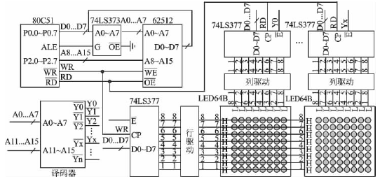
Figure 1 High-speed control scheme LED display electrical principle
There are two characteristics of this solution: First, although the CPU still writes the pattern data of the latch of the column drive circuit through the parallel bus, the latch signal of the latch is changed to the CPU control signal RD instead of the conventional usage WR; Second, the address decoding circuit ensures that the chip select address of the LED dot matrix chip column drive circuit and the logical address of a certain section of the data memory are overlapping, rather than the conventional usage, these two sets of addresses must be separated.
Due to some simple changes in the above circuit, the display control efficiency of the single-chip computer on the LED display screen will change significantly. The specific working process is as follows: Assuming that the data pointer DPTR has been loaded with the address of the data memory, execute the instruction "MOVXA, @DPTR". The function of this instruction is that the CPU reads the font data from the external data memory according to the DPTR and reads it into the accumulator A; but in this circuit, due to the chip select address of the LED dot matrix chip column drive circuit and the data memory The logical addresses of a segment are overlapping, that is to say, when executing the instruction "MOVXA, @DPTR", in addition to pointing to an address in the external data memory, DPTR also selects the latch of a certain LED dot matrix chip drive circuit Device. If the latch pin of the selected latch happens to come in with a pulse, the latch will also lock the font data sent from the external data memory. This pulse is used for RD. RD is the read control signal issued by the CPU to the external data memory when the instruction "MOVXA, @DPTR" is executed. Since the timing of the read control signal RD and the write control signal WR of the MCS51 series of single-chip microcomputers are exactly the same [2], RD replaces WR to achieve the latch function, and of course there is no suspense. When this instruction is executed, it completes the reading of the data memory and also completes the writing of the LED dot matrix, thus speeding up the process of display control.
As mentioned earlier, when the parallel bus is used, the CPU completes the programming process of writing data to the latch of the column drive circuit of the LED dot matrix chip, which takes about ten μs; but now it is only 4 μs, which is much faster, because it is now completed The programming process of writing the mold data to the latch of the column drive circuit of the LED dot matrix once only requires two steps. First, the data pointer DPTR is assigned an effective address, and then the CPU reads the mold data from the external data memory according to the DPTR. At the same time, the font data is also transferred to the latch of the LED dot matrix chip driving circuit. 2 instructions, 4 machine cycles, 4 μs. It is necessary to add a point here, when programming the latch writing data of all LED dot matrix chip drive circuits, do not use cyclic instructions, because then each process has to increase by 2 μs; The method of programming piece by piece, although the program compiled in this way takes up space, but saves time. The design method of using space for time is sometimes a method that designers should try.
The latch control of the row-driven latch of this circuit still uses the write control signal WR of the CPU without change. The chip select signal of the row drive latch also comes from the address decoding circuit. In order to avoid the mutual interference between the data storage and the LED dot matrix, this part of the storage space of the data storage corresponding to this group of addresses is not needed.
The design of the address decoding circuit should ensure that the chip select address of the LED dot matrix chip column drive circuit and the logical address of a certain section of the data memory overlap. Specific design examples are as follows:
Assume that a certain LED display screen uses 240 LED dot matrix chips, which can display 60 Chinese characters of 16 × 16, and a MCS51 series single-chip microcomputer is used for high-speed control. There should be 240 chip select addresses for the 240 LED dot matrix chip column drive circuit. The address decoding circuit must ensure that the effective address after decoding is greater than this number. In the address decoding circuit in FIG. 1, the input address signals are A0 to A7 and A11 to A15, and A8, A9, and A10 are not connected. With the 74LS138 decoder, 256 effective address lines can be obtained after three levels of decoding. The first effective address line corresponds to 8 addresses of the external data memory: 0000H, 0100H, 0200H, 0300H, 0400H, 0500H, 0600H, 0700H. The second effective address line corresponds to the 8 addresses of the external data memory: 0001H, 0101H, 0201H, 0301H, 0401H, 0501H, 0601H, 0701H. ... the 256th effective address line corresponds to the 8 addresses of the external data memory: 00FFH, 01FFH, 02FFH, 03FFH, 04FFH, 05FFH, 06FFH, 07FFH. These 256 effective address lines, 240 chip select addresses for the column drive circuit, and the remaining chip select addresses for the row drive circuit; if not enough, the row drive circuit can be considered to be controlled by a serial bus. The above analysis results show that the I / O interface address of an LED dot matrix chip and the 8-byte address of the data memory establish an overlapping relationship. This is because each LED dot matrix has 8 lines, and each line corresponds to 1 byte of font data.
The above analysis results also show that the mapping relationship is established between the I / O interface addresses of all LED dot matrix chips and the 0000H ~ 07FFH address segment of the data memory. The data memory 0000H ~ 07FFH stores exactly the font data of one frame of image.
4 Application of high-speed control scheme in LED display
The large-screen LED display screens currently used commercially have hundreds, thousands, or even thousands of LED dot matrix chips. The control of the LED display screen by the single-chip computer includes the communication between the single-chip computer and the PC, the data processing of the font data and the display control. A single-chip microcomputer must communicate with a PC, perform data processing, and display control. It must be too busy.
In order to solve the control problem of large-screen LED display screens, many documents have successfully designed the control scheme. The basic idea of ​​many programs [36] is that data processing is done by a single-chip computer, and display control is done by another single-chip computer or a specially designed circuit. Although the control efficiency of these schemes is high, the circuit is relatively complicated.
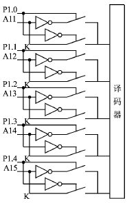
Figure 2 Data memory segment selection switch circuit
The basic idea of ​​this scheme is that the communication, data processing and display control of the single chip microcomputer and the PC are all completed by one single chip microcomputer. The display control uses the high-speed control scheme proposed in this paper, the circuit is simple, and the efficiency of the display control is very high. For example, when the LED dot matrix chip adopts the commonly used 6 cm × 6 cm outer dimension LED dot matrix chip, when the screen area is less than 2 m2, one MCS51 series single-chip microcomputer can be completed. However, the high-speed control scheme is used for large-screen LED displays, and there are still some problems to be solved:
â‘ The communication problem between the SCM and the PC. When the large-screen LED display is connected to the PC, the PC is used to edit the content to be displayed and pass the content to the single-chip computer in the large-screen LED display. When the PC communicates with the SCM, it will not interfere with the work of the display screen. Because the display screen is displayed field by field, there is a black screen time between fields, and there is no problem using the black screen time for communication.
â‘¡ Increase the problem of displaying sessions. Most display screens work in such a way that the content displayed is one cycle after another, and so on. The previous design only considered the problem of establishing a mapping relationship between the I / O interface address of the LED dot matrix and a section of the data memory when displaying a frame of image, so only a freeze image can be displayed. Adding FIG. 2 on the basis of FIG. 1 can make the mapping relationship between the I / O interface address of the LED dot matrix chip and multiple segments of the data memory. When working, the multi-channel switch is controlled by the P1 port to switch the different sections of the data memory and the I / O interface address mapping of the LED dot matrix, so the display screen can be displayed one by one in a loop. If the number of pieces of external data storage is expanded and one of them is enabled by the P1 port, then more segments can be expanded to establish a mapping relationship with the I / O interface address of the LED dot matrix chip. Some display effects such as running water can also be achieved.
â‘¢ The data processing problem of font data. There are many ways to display it, such as freezing, sliding screen, and flowing water. Among the flowing methods, there are leftward flowing water and rightward flowing water. When the display mode is converted, the data processing of the font data must be performed once, and a single-chip microcomputer is used, which will not be a problem. Because when the display mode is switched, the black screen is originally 1 s to several s, and this time just happens to be used for data processing.
Conclusion
The high-speed control scheme of the LED display screen has been proved to be stable and reliable by application, and the circuit is simple, especially suitable for the use of bank exchange rate display screen and interest rate display screen. In addition, the idea of ​​flexible use of reading instructions proposed in this article can also be used as a reference for people.
Protective Face Mask,Anti-particulate Protective Mask,Face Mask KN95,Non Medical Face Mask
Jilin Province Wanhe light Co.,Ltd , https://www.wanhelight.com