White LED lighting has been widely recognized by everyone for its high efficiency, low power consumption, energy saving and environmental protection. In essence, an LED is a illuminable diode whose luminous intensity is proportional to the forward current passing through it and has a turn-on voltage. When the current is 20 mA, the forward voltage drop is generally 3 to 3.5 V. . In many cases, the luminous intensity of a single LED does not meet the needs of practical applications. It is also necessary to use multiple LEDs in series or in parallel, which requires a large voltage or current to drive, and different manufacturing processes, even different batches, LEDs There is a problem of performance mismatch, which also poses a problem for rational design drive. Therefore, although there are many types of original power supplies, they cannot directly supply power to the LEDs. This requires a boost or buck according to different needs, as well as a constant current or constant voltage drive.
1 Common LED driver working principle
1.1 Linear Regulator Driver
The earliest set of linear regulator drivers appeared in the 1970s, when the NPN tube was used as a voltage regulator device, as shown in Figure 1. This regulator requires 2Vbe between the input voltage and the output voltage. When the input voltage is lower than 2Vbe, the NPN tube becomes saturated and the regulator loses its regulation capability. In order to reduce the pressure difference, a combined regulator has appeared. As shown in Fig. 2, the base of the NPN tube is driven by a PNP tube, but the pressure difference is also close to 1 Vbe. In the mid-1980s, low-dropout linear regulators appeared on the market, as shown in Figure 3. Unlike the NPN regulator, the PNP regulator voltage difference is not a function of Vbe, but a function of the PNP tube Vce. This voltage value is much lower. As the manufacturing process matures, the PNP regulator voltage difference is less than 500. mV.
A linear regulator driver is a transistor that operates in a linear or saturation region. The FET removes excess voltage from the input voltage, producing an adjustable, stable, and accurate DC voltage, usually by a voltage regulator, error amplifier, and feedback. Circuit and reference voltage components. The voltage regulator device is usually a MOS transistor, which is equivalent to a voltage-controlled resistor, and the gate voltage controls the size of the resistor. The output voltage Vout is Vout=Vin-Vp obtained by the voltage divider device and the load divider. If the input voltage Vin or the load changes, the control terminal voltage Vc also changes, and the MOS tube resistance value is controlled to adjust the MOS tube voltage division. The purpose of the Vp size is to make Vout stable. The linear regulator driver can also be connected in series with the load. The feedback voltage Vo=Iout×R1 keeps the R1 size unchanged. The feedback voltage can reflect the change of the output current, and then change to a linear steady current driver. The principle of operation is basically the same as that of a linear regulator driver.
The efficiency of a linear regulator is relatively low. It can be known from the principle that the output voltage of the driver is obtained by subtracting the MOS tube voltage division Vp from the input voltage, and this part of the voltage is completely converted into heat energy consumption. Therefore, in order to improve the driver efficiency, it is generally required that the Vp is as low as possible. A linear regulator driver with a low input/output voltage difference is called a low dropout linear regulator, or LDO for short.
1.2 Charge Pump Driver
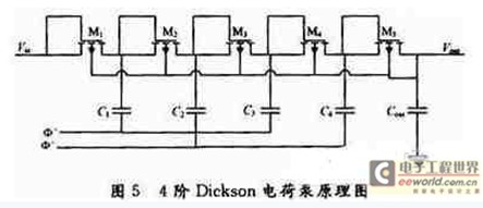
The earliest ideal charge pump model was proposed by Dickson J in 1976. As shown in Figure 5, the basic idea is to generate high voltage through the accumulation effect of capacitance on the charge. Later, Witte-rs J, Toru Tranzawa and others improved the charge pump model of Dickson J, and proposed a more accurate theoretical model, which was confirmed by experiments.
The modern charge pump mainly realizes DC-DC conversion by switch array, oscillating circuit, logic circuit and comparator. The driving mode is also changed from the previous single mode to the adaptive multi-mode. The main form is single mode (such as 2X mode). In dual mode (such as 1X/2X mode) and multi-mode (such as 1X/1.5X/2X mode), the following two-mode 1X/2X charge pump is used to analyze the working principle of the charge pump.
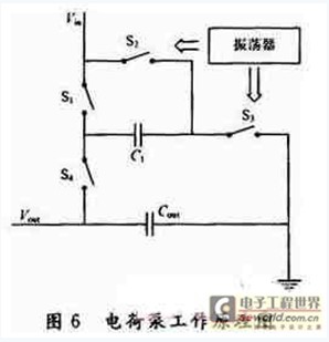
As shown in Figure 6, when the charge pump operates in 1X mode, the oscillator does not work, S1 and S4 are directly turned on, at this time, Vin = Vout; when the charge pump operates in 2X mode, the oscillator output is occupied. The ratio is 50% square wave, so that S1, S3 and S2, S4 are turned on in turn. When the clock signal is high, S1 and S3 are turned on, S2 and S4 are turned off, Vin is connected to C1, and C1 is charged to make Vc =Vin; when the clock signal is low, S1 and S3 are disconnected, S2 and S4 is turned on, Vin is externally powered by C1, so when there is steady state, Vout=Vin+Vc=2Vin.
The charge pump driver circuit not only can effectively boost the buck output, but also can easily carry out the negative voltage output, which is a big advantage of the charge pump driver compared to the other two drivers.
As shown in Figure 7, its basic principle is consistent with the Dickson charge pump, but the voltage difference across the capacitor does not jump. When the circuit is kept in charge and discharge, the voltage difference across the capacitor remains constant. In this case, the original high potential terminal is grounded, so that a negative voltage output can be obtained.
 .
.
Where: Pin is the total input power; Lout is the total current flowing through the load LED; VLED is the forward voltage drop of the LED; M is the boosting multiple of the charge pump; Iq is the drive current of the charge pump power tube and other modules Static current. It can be seen from the above equation that the larger the boosting factor M of the charge pump is, the lower the conversion efficiency of the charge pump is. Therefore, under the condition that the LED driving voltage, that is, Vout>VLED, is satisfied, the charge pump should be operated as low as possible. In the mode of multiples.
1.3 Inductive Switching Regulator Driver
The inductive switching regulator driver is called Switching Power Supply. It is named because the device that adjusts the voltage regulation function in the power supply always works in the switching mode. The early switching power supply frequency was only a few kilohertz. When the frequency reached about 10 kHz, the magnetic components such as transformers and inductors emitted very harsh noise. Until the 1970s, the switching frequency broke the 20 kHz of the human ear's hearing limit. The problem is solved. As the switching frequency continues to increase, the size of the drive is reduced and the efficiency is improved. In the 1980s, zero-voltage and zero-current switching circuits using quasi-resonant technology, namely soft-switching technology, emerged. This circuit makes the voltage and current before the switch is turned on or off is zero, which solves the switching loss and switching noise problem in the circuit, so that the switching frequency can be greatly improved, so that the switching power supply is further small in size and light in weight. High efficiency and high power density.
The core of the inductive switching regulator driver is the electronic switching circuit. According to the output voltage regulation or steady current characteristics of the power supply, the feedback control circuit is used to control the switching circuit. When the switch tube is closed, the energy of the power source is stored in the inductor. When the switch tube is turned off, the energy in the inductor flows into the capacitor, thus realizing the transmission of energy.
The inductive switching regulator driver has two common control modes: one is to maintain the switching cycle of the switch, and the pulse width modulation mode (PWM) that controls the on-time of the switch. When the input voltage or load changes, the control circuit passes. Closed-loop feedback of the difference between the output voltage or current and the reference voltage, adjusting the on-pulse width of the main circuit switching device, so that the output voltage or current of the inductive switching regulator driver remains stable; the other is to keep the on-time unchanged The pulse frequency modulation mode (PFM) for changing the duty cycle of the switch, the basic working principle is that the control circuit performs closed-loop feedback through the difference between the output voltage and the reference voltage under the condition of input voltage or load change, while keeping the switch open time unchanged. In the case of controlling the length of the switching cycle, that is, controlling the switching frequency, the switching duty ratio is adjusted to achieve the purpose of stabilizing the output voltage or current. Since the PWM mode circuit is simple and the input/output range is wider than the PFM method (PFM is usually used for light load, low voltage, and low current), it has been widely used. The following two types of PWM driving methods are mainly introduced.
1.3.1 Voltage Controlled PWM
The structure diagram is shown in Figure 8.
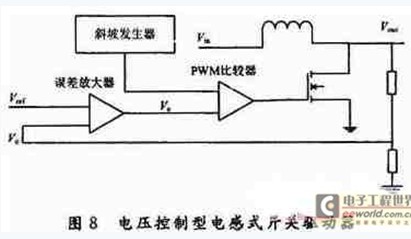
In the PWM controller, the output voltage Vo is detected and applied to the inverting input of the op amp, and the fixed reference voltage Vref is applied to the non-inverting input of the op amp. After the error is amplified, the DC error voltage Ve is output and applied to the non-inverting input of the PWM comparator; the ramp signal generator generates a sawtooth signal Vosc to the inverting input of the PWM comparator. After Vc and Vosc are compared by PWM, a square wave signal is output, and the duty ratio of the square wave signal changes with the error voltage Vc. When the output voltage decreases, the Ve value becomes larger. After the PWM comparison, the output square wave duty ratio decreases, the MOS tube conduction time increases, Vin increases the inductor charging time, and Vout rises.
1.3.2 Current Control PWM Principle
The structure diagram is shown in Figure 9. The difference between the circuit and the voltage control type is that the circuit has two parts of an outer control loop and an inner control loop. When the output current Iout decreases, the error amplifier output increases, the PWM output is 0; when the rising edge of the oscillating wave comes, the MOS transistor is turned on, Vin charges the inductor, the current increases, and the feedback voltage increases through the sampling resistor R3, when the feedback voltage When the value exceeds Ve, the PWM output is 1. When the falling edge of the oscillator comes, the MOS transistor is turned off, and the current on the inductor is output to the outside. The current control mode has the same inverse relationship with the output voltage as the voltage control mode. It also has the following characteristics: the outer control loop controls the current minimum; the inner loop controls the current maximum.

2 Comparison of advantages and disadvantages of various drives
For the LED driving method, each LED driver has its applicable range, and also has its own advantages and disadvantages, to understand their respective advantages and disadvantages, and to better design a reasonable LED driving circuit according to the actual situation, which can be passed Efficiency White LED lighting has been widely recognized by everyone for its high efficiency, low power consumption, energy saving and environmental protection. In essence, an LED is a illuminable diode whose luminous intensity is proportional to the forward current passing through it and has a turn-on voltage. When the current is 20 mA, the forward voltage drop is generally 3 to 3.5 V. . In many cases, the luminous intensity of a single LED does not meet the needs of practical applications. It is also necessary to use multiple LEDs in series or in parallel, which requires a large voltage or current to drive, and different manufacturing processes, even different batches, LEDs There is a problem of performance mismatch, which also poses a problem for rational design drive. Therefore, although there are many types of original power supplies, they cannot directly supply power to the LEDs. This requires a boost or buck according to different needs, as well as a constant current or constant voltage drive.
1 Common LED driver working principle
1.1 Linear Regulator Driver
The earliest set of linear regulator drivers appeared in the 1970s, when the NPN tube was used as a voltage regulator device, as shown in Figure 1. This regulator requires 2Vbe between the input voltage and the output voltage. When the input voltage is lower than 2Vbe, the NPN tube becomes saturated and the regulator loses its regulation capability. In order to reduce the pressure difference, a combined regulator has appeared. As shown in Fig. 2, the base of the NPN tube is driven by a PNP tube, but the pressure difference is also close to 1 Vbe. In the mid-1980s, low-dropout linear regulators appeared on the market, as shown in Figure 3. Unlike the NPN regulator, the PNP regulator voltage difference is not a function of Vbe, but a function of the PNP tube Vce. This voltage value is much lower. As the manufacturing process matures, the PNP regulator voltage difference is less than 500. mV.
A linear regulator driver is a transistor that operates in a linear or saturation region. The FET removes excess voltage from the input voltage, producing an adjustable, stable, and accurate DC voltage, usually by a voltage regulator, error amplifier, and feedback. Circuit and reference voltage components. The voltage regulator device is usually a MOS transistor, which is equivalent to a voltage-controlled resistor, and the gate voltage controls the size of the resistor. The output voltage Vout is Vout=Vin-Vp obtained by the voltage divider device and the load divider. If the input voltage Vin or the load changes, the control terminal voltage Vc also changes, and the MOS tube resistance value is controlled to adjust the MOS tube voltage division. The purpose of the Vp size is to make Vout stable. The linear regulator driver can also be connected in series with the load. The feedback voltage Vo=Iout×R1 keeps the R1 size unchanged. The feedback voltage can reflect the change of the output current, and then change to a linear steady current driver. The principle of operation is basically the same as that of a linear regulator driver.
The efficiency of a linear regulator is relatively low. It can be known from the principle that the output voltage of the driver is obtained by subtracting the MOS tube voltage division Vp from the input voltage, and this part of the voltage is completely converted into heat energy consumption. Therefore, in order to improve the driver efficiency, it is generally required that the Vp is as low as possible. A linear regulator driver with a low input/output voltage difference is called a low dropout linear regulator, or LDO for short.
1.2 Charge Pump Driver
The earliest ideal charge pump model was proposed by Dickson J in 1976. As shown in Figure 5, the basic idea is to generate high voltage through the accumulation effect of capacitance on the charge. Later, Witte-rs J, Toru Tranzawa and others improved the charge pump model of Dickson J, and proposed a more accurate theoretical model, which was confirmed by experiments.
The modern charge pump mainly realizes DC-DC conversion by switch array, oscillating circuit, logic circuit and comparator. The driving mode is also changed from the previous single mode to the adaptive multi-mode. The main form is single mode (such as 2X mode). In dual mode (such as 1X/2X mode) and multi-mode (such as 1X/1.5X/2X mode), the following two-mode 1X/2X charge pump is used to analyze the working principle of the charge pump.
As shown in Figure 6, when the charge pump operates in 1X mode, the oscillator does not work, S1 and S4 are directly turned on, at this time, Vin = Vout; when the charge pump operates in 2X mode, the oscillator output is occupied. The ratio is 50% square wave, so that S1, S3 and S2, S4 are turned on in turn. When the clock signal is high, S1 and S3 are turned on, S2 and S4 are turned off, Vin is connected to C1, and C1 is charged to make Vc =Vin; when the clock signal is low, S1 and S3 are disconnected, S2 and S4 is turned on, Vin is externally powered by C1, so when there is steady state, Vout=Vin+Vc=2Vin.
The charge pump driver circuit not only can effectively boost the buck output, but also can easily carry out the negative voltage output, which is a big advantage of the charge pump driver compared to the other two drivers.
As shown in Figure 7, its basic principle is consistent with the Dickson charge pump, but the voltage difference across the capacitor does not jump. When the circuit is kept in charge and discharge, the voltage difference across the capacitor remains constant. In this case, the original high potential terminal is grounded to obtain a negative voltage output.
Where: Pin is the total input power; Lout is the total current flowing through the load LED; VLED is the forward voltage drop of the LED; M is the boosting multiple of the charge pump; Iq is the drive current of the charge pump power tube and other modules Static current. It can be seen from the above equation that the larger the boosting factor M of the charge pump is, the lower the conversion efficiency of the charge pump is. Therefore, under the condition that the LED driving voltage, that is, Vout>VLED, is satisfied, the charge pump should be operated as low as possible. In the mode of multiples.
1.3 Inductive Switching Regulator Driver
The inductive switching regulator driver is called Switching Power Supply. It is named because the device that adjusts the voltage regulation function in the power supply always works in the switching mode. The early switching power supply frequency was only a few kilohertz. When the frequency reached about 10 kHz, the magnetic components such as transformers and inductors emitted very harsh noise. Until the 1970s, the switching frequency broke the 20 kHz of the human ear's hearing limit. The problem is solved. As the switching frequency continues to increase, the size of the drive is reduced and the efficiency is improved. In the 1980s, zero-voltage and zero-current switching circuits using quasi-resonant technology, namely soft-switching technology, emerged. This circuit makes the voltage and current before the switch is turned on or off is zero, which solves the switching loss and switching noise problem in the circuit, so that the switching frequency can be greatly improved, so that the switching power supply is further small in size and light in weight. High efficiency and high power density.
The core of the inductive switching regulator driver is the electronic switching circuit. According to the output voltage regulation or steady current characteristics of the power supply, the feedback control circuit is used to control the switching circuit. When the switch tube is closed, the energy of the power source is stored in the inductor. When the switch tube is turned off, the energy in the inductor flows into the capacitor, thus realizing the transmission of energy.
The inductive switching regulator driver has two common control modes: one is to maintain the switching cycle of the switch, and the pulse width modulation mode (PWM) that controls the on-time of the switch. When the input voltage or load changes, the control circuit passes. Closed-loop feedback of the difference between the output voltage or current and the reference voltage, adjusting the on-pulse width of the main circuit switching device, so that the output voltage or current of the inductive switching regulator driver remains stable; the other is to keep the on-time unchanged The pulse frequency modulation mode (PFM) for changing the duty cycle of the switch, the basic working principle is that the control circuit performs closed-loop feedback through the difference between the output voltage and the reference voltage under the condition of input voltage or load change, while keeping the switch open time unchanged. In the case of controlling the length of the switching cycle, that is, controlling the switching frequency, the switching duty ratio is adjusted to achieve the purpose of stabilizing the output voltage or current. Since the PWM mode circuit is simple and the input/output range is wider than the PFM method (PFM is usually used for light load, low voltage, and low current), it has been widely used. The following two types of PWM driving methods are mainly introduced.
1.3.1 Voltage Controlled PWM
The structure diagram is shown in Figure 8.
In the PWM controller, the output voltage Vo is detected and applied to the inverting input of the op amp, and the fixed reference voltage Vref is applied to the non-inverting input of the op amp. After the error is amplified, the DC error voltage Ve is output and applied to the non-inverting input of the PWM comparator; the ramp signal generator generates a sawtooth signal Vosc to the inverting input of the PWM comparator. After Vc and Vosc are compared by PWM, a square wave signal is output, and the duty ratio of the square wave signal changes with the error voltage Vc. When the output voltage decreases, the Ve value becomes larger. After the PWM comparison, the output square wave duty ratio decreases, the MOS tube conduction time increases, Vin increases the inductor charging time, and Vout rises.
1.3.2 Current Control PWM Principle
The structure diagram is shown in Figure 9. The difference between the circuit and the voltage control type is that the circuit has two parts of an outer control loop and an inner control loop. When the output current Iout decreases, the error amplifier output increases, the PWM output is 0; when the rising edge of the oscillating wave comes, the MOS transistor is turned on, Vin charges the inductor, the current increases, and the feedback voltage increases through the sampling resistor R3, when the feedback voltage When the value exceeds Ve, the PWM output is 1. When the falling edge of the oscillator comes, the MOS transistor is turned off, and the current on the inductor is output to the outside. The current control mode has the same inverse relationship with the output voltage as the voltage control mode. It also has the following characteristics: the outer control loop controls the current minimum; the inner loop controls the current maximum.
2 Comparison of advantages and disadvantages of various drives
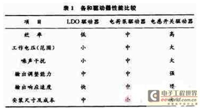
For the LED driving method, each LED driver has its applicable range, and also has its own advantages and disadvantages, to understand their respective advantages and disadvantages, and to better design a reasonable LED driving circuit according to the actual situation, which can be passed Comparison of efficiency operating voltage, noise interference, output regulation, reaction speed, and installation size and cost.
Comparative analysis of operating voltage, noise interference, output regulation, reaction speed, and installation size and cost.
2.1 Overall efficiency
The overall efficiency of the linear regulator driver is relatively low, mainly because the linear regulator driver relies on the power tube to remove excess voltage to achieve the voltage regulation effect, and this part of the power consumption is completely useless, resulting in a decrease in driver efficiency. . Therefore, when using a linear regulator driver, the input and output voltage difference should be minimized. The actual conversion efficiency is usually between 50% and 95%. Since the basic charge pump can only provide multiple output voltages, its output voltage cannot be stabilized at some Value, so usually add extra LDO outside the charge pump circuit, convert to a regulated charge pump, which leads to the charge pump driver efficiency based on its own power sheath consumption, additional power consumption of the LDO driver, efficiency Usually 70% to 85%; the loss of the inductive switch driver and the basic charge pump driver mainly comes from the static current loss of the internal MOS device, the external capacitor and the power loss of the sampling resistor, and the efficiency can reach 80% to 90%.
2.2 Working voltage
Due to the voltage division operation principle, the linear regulator driver can only perform the buck output, which determines that it can only work when the input voltage is higher than the LED drive demand voltage; the charge pump driver can be stepped down or boosted. However, if high-multiplier or multi-mode adjustment of the output voltage is required, a large number of switches and capacitors need to be connected, so that the efficiency is greatly reduced, so it is generally applied to excessive voltage driving, that is, a case where the input voltage and the output LED driving voltage are not significantly different; Inductive switch driver utilizes magnetic field energy storage, whether it is boost, buck or both, just adjust the ratio of the sampling resistor to make a wide range of output voltage adjustment, and will not change the driver due to output adjustment. Efficiency, so it has the widest application range and can be widely used under various input voltages.
2.3 Noise Interference (EMI)
Due to its working principle, the linear regulator driver stabilizes the output voltage by means of voltage division. It does not require capacitors or inductors for voltage regulation. The MOS transistor always works in a linear state and does not need to be turned off or turned on. No noise voltage, current and electromagnetic interference will occur; the charge pump does not use inductance, so its EMI effect can be neglected. In the process of output voltage, MOS tube needs to be switched, so it will generate certain power supply noise, but because there is no The use of inductors, so the noise is small, can be eliminated by a small external capacitor; inductive switch driver is the main source of power supply noise and EMI, due to the frequent switching operation of MOS tube, PWM will be generated in the fixed frequency of MOS tube switch Large EMI interference, PFM is more likely to cause interference in the variable range of its frequency, so suppliers usually need to improve the operating frequency of the inductive switch, so that its EMI falls outside the system band, and because of the inductance, When the MOS tube is turned on and off, a large peak current or voltage is generated, and the output current and voltage also exist.
2.4 Output adjustment and response speed
The linear regulator driver can adjust the voltage division of the MOS tube according to the needs of the product, adjust the voltage division of the MOS tube, control the output voltage, and the circuit is simple and the response speed is fast; the charge pump driver itself cannot adjust the output voltage at will. The value can only be adjusted by the sampling voltage feedback. The voltage adjustment can also be performed by serially connecting the LDO, but this will also reduce the response speed of the driver. The response speed is slower than that of the LDO. The advantage of the charge pump for adjusting the output voltage is that it can By simple design, the positive and negative voltages are output, and the other two driving modes require another design circuit to achieve the output negative voltage effect; the inductive switch driver only adjusts the sampling resistor for the output voltage adjustment. The ratio is changed to control the square wave duty cycle to adjust the output voltage. The adjustment is relatively simple. However, due to the complicated circuit structure, multiple comparison and amplification are required. The presence of the inductor further slows down the response speed of the voltage adjustment, so the response speed. slowest.
2.5 Installation size and cost
The linear voltage regulator driver circuit is simple in structure, generally only needs 20 to 40 components, and the cost is low. However, since the MOS tube is always in a linear region or a saturated region, the heat generation is large, so a large heat sink is required. To ensure good heat dissipation and ensure system stability. The charge pump circuit is moderately complex, and the external capacitor volume can also be reduced by increasing the switching frequency. Now, the chip capacitor is also well applied, which greatly increases the charge pump integration and further reduces the required mounting size. . Inductive switch driver circuits are the most complex and costly, and require at least one external inductor, capacitor, and Schottky diode. Especially when shielding applications are required, additional shields are required for higher cost and larger size. The attached table is shown in Table 1.
3 LED lighting practical circuit application
After understanding the working principle, advantages and disadvantages of various drivers, we can easily classify and summarize some common LED lighting driver circuits.
3.1 Lithium battery powered LED driver
Lithium battery voltage is usually between 2.5 and 4.5 V. It is usually portable equipment powered by lithium battery, including mobile phone, MP4, laptop, etc. For the convenience of carrying, the device is small in size, light in weight, and highly integrated. Large electromagnetic interference can affect other circuits. According to the actual situation of portable equipment, LED driver needs to meet the following requirements: boost drive; small footprint; low electromagnetic interference; high conversion efficiency. Small device LCD lighting only needs to use 3 to 9 LEDs in series and parallel, but has high requirements for luminous consistency. Large device LCD lighting usually takes the form of a backlight module. The backlight module has processed the white light LED source through refraction, light guiding and other process technologies to deal with the problem of light uniformity. Therefore, the consistency requirement for luminescence is low. The optimal circuit structure is a charge pump drive mode with an LDO. This drive mode can boost, occupy a small area, and has low EMI interference.
3.2 Battery powered LED driver
The battery voltage is usually between 12 and 36 V. The input voltage is always higher than the LED tube voltage drop. In this case, only the step-down operation can be performed, such as solar street lights and motor vehicle lighting systems. This situation tends to have lower requirements for LED illumination; however, for high luminance requirements, high-power LEDs are often used, and the best solution is to take advantage of the highest efficiency and low cost. Inductive switch driver.
3.3 General lighting applications in the case of utility power
Mains power supply is the most meaningful kind of power supply for LED lighting. It is an application that determines whether LED can be truly popularized. Therefore, it is an important issue that LED lighting must study and solve. Power supply from the mains supply, the primary solution is the buck, rectification problem, while taking into account the LED drive power will have an impact on the power grid, but also to solve the problem of power supply noise, electromagnetic interference and high power factor, so the circuit isolation method is required. Reduce pollution to the grid. For small and medium power LEDs, the best circuit structure is an isolated single-ended flyback converter. Due to the limited output power capability of single-ended flyback circuits, bridge switching converters with larger output power should be used for applications above several hundred watts.
4 Conclusion
With the rapid development of portable devices and the maturity of commercial power LED lighting technology, more and more devices use LED lighting, and the demand for LED driving chips will be further expanded. In short, the use of white LEDs is very extensive, and the design of the driver circuit is very critical. Only for different application environments and reasonable driving methods can the most stable and reasonable driving circuit be designed in practical applications.
Our factory was set up in 2001. Electric Food Chopper is our main products. Food Chopper have all kind of lite for you to choose, such as:0.6l, 0.7L,1.0L,1.5L,2.0L. In addition, there are tow kinds material of bowl, one is plastic another one is glass. What's more, the motor of our Household Food Chopper are all full copper motor. And we have different blade , such as single blade, double blade,triple blade and rubber blade. There is no doubt that customers have a variety of choices. Kitchen food chopper is good quality.
Food Chopper
Meat Chopper,Vegetable Dicer,Garlic Chopper,Kitchenaid Chopper
JIANGMEN JIANGHAI DISTRICT SHENGHUI ELECTRIC CO.,LTD , https://www.shenghuielectric.com