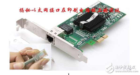
The network interfaces we use today are all Ethernet interfaces, and most processors currently support Ethernet ports. At present, Ethernet mainly includes 10M, 10/100M, and 1000M interfaces, and 10M applications are few and basically replaced by 10/100M. At present, the Ethernet interface type of our products mainly adopts the twisted pair RJ45 interface, and is basically applied in the field of industrial control. Due to the particularity of the industrial control field, we have considerable research on Ethernet device selection and PCB design. From the hardware point of view, the Ethernet interface circuit is mainly composed of MAC (Media Access Controlleroler) control and physical layer interface (Physical Layer, PHY). Most processors contain Ethernet MAC control internally, but do not provide a physical layer interface. Therefore, an external physical chip is required to provide an Ethernet access channel. Faced with such a complicated interface circuit, I believe that hardware engineers want to know how the hardware circuit is implemented on the PCB.
Figure 1 below shows a typical application of Ethernet. Our PCB design is basically laid out according to this block diagram. Below we will use this block diagram to explain the Ethernet-related layout and wiring points.
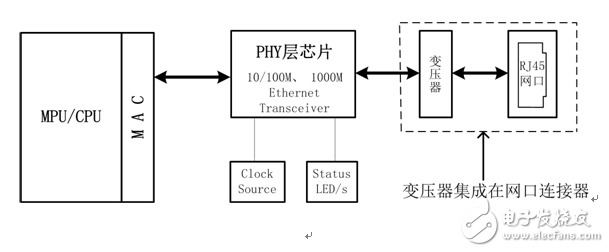
Figure 1 Typical Ethernet application
1. Figure 2 Network port transformer does not have the PCB layout and wiring diagram of the reference circuit integrated in the network port connector. The following points are to be noted in Figure 2 for the layout and wiring of the Ethernet circuit.
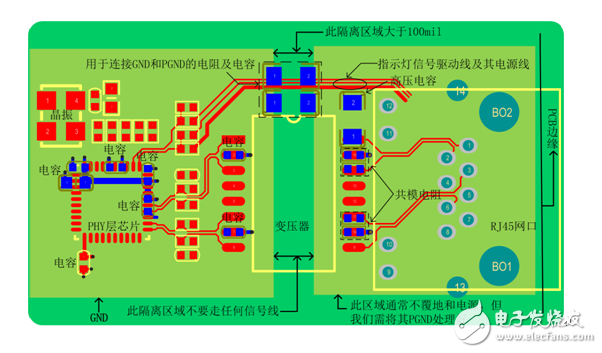
Figure 2 Transformer does not have a circuit PCB layout and wiring reference integrated in the network port connector
a) The distance between the RJ45 and the transformer is as short as possible. The crystal oscillator is far from the interface, the edge of the PCB and other high-frequency devices, traces or magnetic components. The distance between the PHY layer chip and the transformer is as short as possible, but sometimes Considering the overall layout, this may be difficult to satisfy, but the distance between them is about 10~12cm. The principle of device layout is usually placed according to the signal flow direction, and must not be circumvented;
b) The power supply filtering of the PHY layer chip is designed according to the requirements of the chip. Usually, a decoupling capacitor is required for each power supply terminal. They can provide a low impedance path for the signal, reduce the resonance between the power supply and the ground plane, in order to make the capacitor Decoupling and bypassing function, so ensure that the loop area composed of capacitors, traces, vias, and pads is as small as possible for the decoupling and bypass capacitors, and the lead inductance is kept as small as possible;
c) Network port transformer PHY layer chip side center tap to the ground filter capacitor should be as close as possible to the transformer pin, to ensure the shortest lead, the smallest distributed inductance;
d) The common mode resistance and high voltage capacitance of the interface side of the network port transformer are placed close to the center tap, and the trace is short and thick (≥15 mil);
e) The two sides of the transformer need to be cut: the RJ45 connector and the secondary winding of the transformer are separated by a separate isolation ground with an isolation area of ​​100 mils or more, and no power and ground layers exist under this isolation area. In this way, the segmentation process is to achieve the primary and secondary isolation, and the interference at the control source is coupled to the secondary through the reference plane;
f) Connect the power cable of the indicator light and the drive signal line adjacent to each other to minimize the loop area. The indicator light and the differential line should be separated as necessary. The two must ensure sufficient distance. If there is space, it can be separated by GND.
g) The resistors and capacitors used to connect GND and PGND should be placed in the divided area.
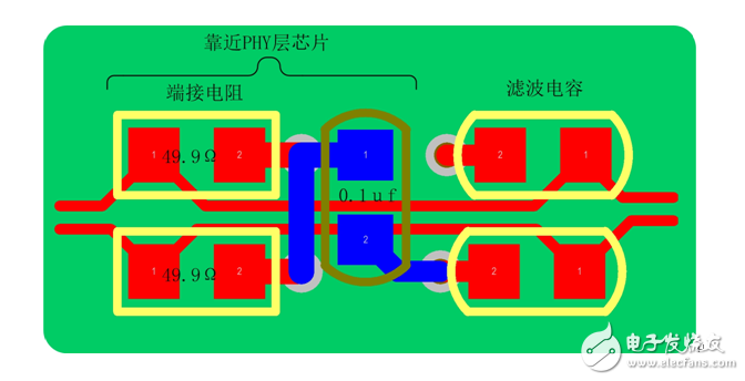
2. The signal line of Ethernet exists in the form of differential pair (Rx±, Tx±). The differential line has strong common-mode rejection and strong anti-interference ability. However, if the wiring is improper, it will bring serious signal integrity. Sexual problems. Let's take a look at the processing points of the differential line:
a) Px±, Tx± differential pairs are drawn first. Try to keep the differential pairs parallel, equal length and short distance to avoid vias and crossovers. Due to factors such as pin distribution, vias, and trace space, the length of the differential line is mismatched, the timing shifts, and common mode interference is introduced to reduce signal quality. Therefore, the corresponding compensation for the mismatch of the differential pair is made to match the line length, and the length difference is usually controlled within 5 mils. The compensation principle is where the length difference compensation occurs;
b) When the speed requirement is high, the Rx±, Tx± differential pair impedance control is required, usually the impedance is controlled at 100Ω±10%;
c) The differential signal termination resistor (49.9Ω, some PHY layer chips may not) must be placed close to the Rx±, Tx± pins of the PHY layer chip, which can better eliminate the signal reflection in the communication cable;
d) The filter capacitors on the differential pair must be placed symmetrically. Otherwise, the differential mode may be converted to common mode, which brings common mode noise, and there is no stub in the trace, so that it can have good suppression of high frequency noise.
3. The PCB layout and wiring of the transformer integrated in the Ethernet circuit of the connector are relatively simple. The following figure 3 is the PCB layout and wiring reference diagram of the network port circuit using the integrated connector:
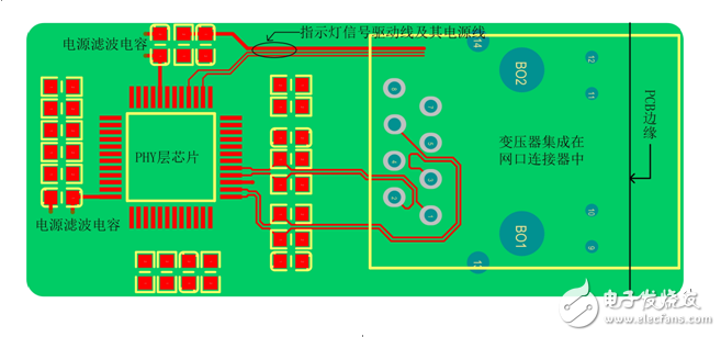
Figure 3 Integrated connector network port PCB layout, wiring reference diagram
As can be seen from the above figure, the difference between Figure 3 and Figure 1 is that there is less network port transformer, and the others are basically the same. The difference is mainly reflected in the fact that the network port transformer has been integrated into the connector, so the ground plane does not need to be split, but we still need to connect the outer casing of the integrated machine to the continuous ground plane.
Ethernet layout and wiring should be roughly the same, good PCB layout and routing can not only ensure circuit performance, but also improve circuit performance, the author's level is limited, the lack of welcome to correct communication.
RJ45 Jack.China RJ45 Jack Crimping,RJ45 Jack Datasheet,RJ45 Connectors HSN Code,RJ45 Connectors 100 Pack Price, we offered that you can trust. Welcome to do business with us.
Antenk Modular Jacks are a complete line of PCB and wire leaded jacks which are UL and CSA approved and meet all required FCC rules and regulations. Antenk offers a multitude of sizes (4P2C thru 10P10C) with styles including single, ganged and stacked versions with options of ferrite or magnetic filtering and or metal shielding. Jacks with integral LED`s,These jacks are available in thru-hole or SMT mounting.
RJ45 interface can be used to connect RJ-45 connectors. It is suitable for the network constructed by twisted pair. This port is the most common port, which is generally provided by Ethernet hub. The number of hubs we usually talk about is the number of RJ-45 ports.
RJ45 is a type of different connectors (for example: RJ11 is also a type of connector, but it is used on the telephone); there are two different ways to arrange the RJ-45 connector: one is white orange, orange, white green, blue, white blue, green, white brown, brown; the other is white green, green, white orange, blue, white blue, orange, white brown, brown; therefore, there are also wires with RJ45 connector There are two kinds: straight line and interleaved line.
The RJ-45 port of the hub can be directly connected to terminal devices such as computers and network printers, and can also be connected with other hub equipment and routers such as switches and hubs. It should be noted that when connecting to different devices, the jumper method of twisted pair cable used is different.
59 Modular Jack
RJ45 Jack Crimping,RJ45 Jack Datasheet,RJ45 Connectors HSN Code,RJ45 Connectors 100 Pack Price
ShenZhen Antenk Electronics Co,Ltd , https://www.antenk.com