Radio Frequency Identification (RFID) technology is a non-contact automatic identification technology based on the principle of radio frequency. Its basic principle is that the signal is transmitted through spatial coupling (alternating magnetic field and electromagnetic field), and this information is generally loaded in the electronic tag. The data format of the information typically has standard Wiegand signals or various serial communication interface signals.
Currently, the application of readers is becoming more and more widespread. In the process of production and sales, people often suffer from a quick and simple method to visually display the output signal of the reader, so that in the production, it is often necessary to rework the product and recalibrate the signal output of the product. In order to solve this problem, the SPCE061A single-chip microcomputer with voice processing function is used as a controller to analyze and process the common output signals of the RF reader.
1 Overall design of the signal analysis systemIn RF readers, common signals that need to be analyzed and processed include RS-232 signals, rs-485/'target='_blank'>RS-485, and Wiegand signals. For the processing of these signals, the Lingyang SPCE061A microcontroller can be used. Sunplus SPCE061A MCU has the common functions of 51 MCU, and the on-chip resources are highly integrated, such as ADC, DAC, RAM, FLASH, timer, phase-locked loop, low voltage detection and reset, watchdog, ICE interface, etc. SPCE061A embeds 32K words of flash memory, and its u'nSP instruction system also provides 16-bit & TImes with higher processing speed; 16-bit multiplication operation instructions and inner product operation instructions, which can easily and quickly process various complex digital signals. Therefore, the system uses SPCE061A as the core control circuit for peripheral circuit development. The overall block diagram of the system is shown in Figure 1.
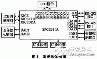
In this system, in order to select the type of data to be tested, a data switching button is designed in the system to enable the system to select and process the read data, and at the same time, in order to visually see the data signal to be analyzed, an LCD is set in the system. The LCD can display the ID of the read data, and the system can alarm the read error ID through the voice module. This article focuses on the use of SPCE061A to analyze and process common signals such as RS-485 and Wiegand signals.
1.1 RS-485 data signal processing
The data frame format of the RS-485 signal to be processed in this paper is as follows:
1 data start flag STX=02H, data end flag ETX=03H.
2DATA is the number of the electronic tag to be read, and the length is 8 bytes of ASCII code. The data is divided into groups of 4 bits in order from highest to lowest, and the value of the 4-bit binary number is represented by ASCII code. Since the 4-bit binary number ranges from 0H to FH, the converted ASCII code is 30H to 39H and 41H to 46H. For example, the 32-bit numbered data is 6A90F103H, which is converted to 8-byte ASCII code and is "36H 41H39H 30H 46H 31H 30H 33H".
3BCC is the check code, which is the result of "exclusive OR" of each byte from STX to ETX. When receiving, the SPCE061A MCU performs a checksum calculation on the received data, and then compares it with the check code to make a bit error judgment.
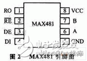
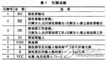
When using the SPCE061A microcontroller to analyze the RS-485 signal, Maxim's MAX481 is used as the RS-485 driver chip. The chip integrates a driver and a receiver, which is compliant with RS-422A and RS-485 communication standards. The MAX481 pin is shown in Figure 2. The pin functions are listed in Table 1.
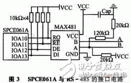
The interface circuit of SPCE061A and RS-485 is shown in Figure 3.
Dual Mining Power Supply 1800W
Specifications:
Item name: Dual Ethereum Mining Power Supply 1800W
Input Voltage: AC 180V~240V
Support graphics card :8
Color: Black
Size: 15 x 14 x 8.6cm
Rated power: 1800W
High Performance of Computing,10% Higher Than Same Level Motherboards.
Equipped Sodimm DDR3 Memory Slot,8*6PIN PCIE X16 Power Supply Socket,Significantly Improve Motherboard Performance.
The Voltage Stabilizing Capacitor Can Provide A Stable Voltage for Your Power Supply Equipment.
It Can Ensure Quiet Performance, Low Power Consumption, Less Heat Generation, Energy Saving and Safe Use.
Features:
The power supply is 1800W conversion efficiency of 90+
Support graphics card 8, video card 6+2pin 16
Gold medal stability is strong
Gifts: power line 1:1 distribution
Voltage : 180v-220v 50Hz 10A
DC OUTPUT: 12V---150A MAX
POWER IN : 2000W MAX
Specification:
Name:Mine Chassis Power Supply
voltage : 180v-264v
Specifications
Color:black
PFC Type:active PFC
Power: max power 2000W
Appropriate Type:Ethereum Mining Power Supply 1800W
best mining psu,mining rig power supply,server power supply for mining,psu for mining rig,power supply for 8 gpu mining rig
Easy Electronic Technology Co.,Ltd , https://www.yxpcelectronicgroups.com