Most large embedded systems are powered by a 48V input that is distributed through the backplane to each printed circuit board in the system. This power delivery method is commonly known as a distributed power system. The 48V input is first converted to a lower intermediate voltage using an isolated intermediate bus converter (IBC), typically ranging from 5V to 12V. This intermediate voltage then needs to be further reduced to supply the branch circuits and integrated circuits (ICs) on the board. These ICs often require current levels ranging from tens of milliamps to tens of amps, with voltages as low as 0.8V or higher. The components responsible for this final voltage reduction are known as point-of-load (POL) regulators.
Distributed power systems often include microprocessors and digital signal processors (DSPs), which have specific power requirements for their core and I/O sections. During startup and shutdown, these power supplies must be carefully sequenced to meet the manufacturer’s specifications. Designers need to manage the relative voltage levels and timing between the core and I/O supplies to prevent damage to the processor or connected devices like memory, FPGAs, or data converters. Improper sequencing can lead to latch-up or excessive current draw, potentially damaging the I/O ports. To avoid this, it's essential to track the core and I/O voltages so that the core is properly biased before the I/O load is applied.
Some processors require the I/O voltage to rise before the core voltage, while others demand the opposite. This variability means that power sequencing is crucial. In complex systems, such as those using application-specific integrated circuits (ASICs), up to seven different voltage rails may need to be controlled in sequence. An ideal power sequencer allows for flexible control over all rails, ensuring that if one rail fails to reach its target voltage during startup, the process halts to prevent damage. Additionally, many processors include internal ESD diodes between the core and I/O supplies. If the voltage isn't properly managed, these diodes could be damaged during power-up or power-down due to reverse current flow.
Pre-biased loads are common in systems where a voltage has already been applied to the load, either in a steady state or during power transitions. ASICs are a typical example, often requiring multiple rails such as 1.0V, 1.1V, 1.2V, 1.8V, 2.5V, and 3.3V. Inside the ASIC, there are internal diodes that protect against overvoltage. However, during power-up or power-down, the voltage difference between two rails might exceed the diode’s breakdown voltage, causing a dangerous current spike that could damage the device. This issue can be mitigated by using a DC/DC converter that prevents negative current flow through the output inductor. This is typically achieved by operating in Burst Mode or Discontinuous Conduction Mode (DCM) during power transitions.
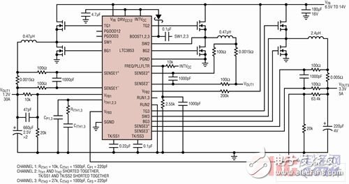
Linear Technology has introduced a new solution for handling pre-biased loads with its LTC3853, a three-output, multi-phase synchronous DC/DC controller. This high-efficiency regulator supports consistent or proportional tracking, making power sequencing straightforward. With an input range of 4.5V to 24V (up to 28V), it is well-suited for most intermediate bus applications. Each of the three output channels can operate independently, with output voltages ranging from 0.8V to 13.5V for one channel and 0.8V to 5.5V for the other two. The controller can deliver more than 20A of total output current and features a constant frequency architecture with programmable PLL synchronization from 250kHz to 750kHz.
The LTC3853 can be configured as three separate outputs or in a 2 + 1 mode, where two channels are combined in parallel for higher current delivery, and the third operates independently. By introducing a 120° phase shift between the three output stages, the controller minimizes noise and improves efficiency. When used in a 2 + 1 configuration, the two main channels are 180° out of phase, ensuring balanced input current distribution even when the output current varies significantly.
Figure 1 shows a dual-output converter operating within a 6.5V to 14V input range. Channels 1 and 2 both provide a 1.2V output, while Channel 3 supplies a 3.3V output. In this 2 + 1 setup, only one RUN pin (RUN1) is needed to start both Channels 1 and 2. The feedback amplifier for Channel 2 is disabled, and the two channels share the same feedback divider from Channel 1. The post-package trim of the current sense comparator ensures excellent current sharing between the two channels. As shown in Figure 2, the inductor current for each channel remains well-balanced, with a transient voltage of less than ±3% under a ±25% load step.
home energy storage,household power storage,home solar power,all in one system
Enershare Tech Company Limited , https://www.enersharepower.com