1 Overview
Frequency synthesis technology is a new technology in the development of modern radio technology and one of the key technologies in modern communication systems. It usually uses a crystal or a small number of crystals to form a standard frequency source, and then generates various required frequencies through a synthesis method. signal. These frequency signals have the same frequency stability and accuracy as standard frequency sources. Circuits constructed using this technique are called frequency synthesizers in communication equipment. There are many types of frequency synthesizers, and digital frequency synthesizers are currently commonly used. The digital frequency synthesizer is composed of crystal oscillator, fixed frequency divider, phase discriminator, filter and VCO, etc. 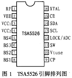 The frequency signal output by the crystal oscillator gets the standard frequency after the fixed frequency divider, and the frequency signal output by the VCO gets the actual frequency signal after the frequency is divided by the variable frequency divider. The circuit lock control voltage will be added to the VCO through the filter to control and correct the actual frequency signal until the loop is locked. When the required signal frequency is high, the design, production, and debugging of the circuit is difficult, and it can usually only be completed by professional manufacturers. Not only is the cost high, but also the production cycle is long. The TSA5526 chip is a general-purpose digital frequency synthesis integrated circuit introduced by Philips. It integrates crystal oscillator, fixed frequency divider, phase discriminator, filter and other circuits on a single chip. Its main characteristics are as follows:
◠The frequency of the input radio frequency signal is: 64 ~ 1300MHz;
â— The level of the input RF signal is: ï¼28 ~ 3dBm;
◠The output error adjustment voltage is: 4.5 ~ 33V;
â— With lock detection function;
â— Built-in programmable 15bit frequency divider;
â— Through program control, the reference signal frequency division ratio can be selected in 512, 640 and 1024. When an external 4MHz crystal oscillator is connected, the frequency accuracy of 3.906625kHz, 6.25kHz and 7.8125kHz can be obtained;
â— I2C bus and 3 bus can be selected for data transmission;
â— Using single power supply, the power supply voltage is 4.5 ~ 5.5V.
2 Pin function
TSA5526 is available in SSO16 and SO16 packages. The pin arrangement is shown in Figure 1. The functions of each pin are listed in Table 1.
Table 1 TSA5526 pin functions
| Lead | Name | Features | Application Instructions |
| 1 | RF | RF signal RF input | Usually connected to local oscillator output |
| 2 | VEE | Ground | |
| 3 | VCC1 | Power supply voltage 1 | Chip power supply, connect to + 5V |
| 4 | VCC2 | Power supply voltage 2 | Switch control power supply, usually + 12V |
| 5 | BS4 | Electronic switch BS4 output | PNP transistor OC output |
| 6 | BS3 | Electronic switch BS3 output | PNP transistor OC output |
| 7 | BS2 | Electronic switch BS2 output | PNP transistor OC output |
| 8 | VS1 | Electronic switch BS1 output | PNP transistor OC output |
| 9 | CP | Loop filter | External RC filter network |
| 10 | Vtune | Error control voltage output | Output the DC voltage through the pull-up resistor and add it to the VCO |
| 11 | SW | Bus select switch | Choose I2C bus mode when grounding; choose 3 bus mode when floating |
| 12 | LOCK / ADC | Lock flag / ADC input | 3 is the lock flag in bus mode, low level is effective; 5 is the level ADC input terminal in I2C bus mode |
| 13 | SCL | Serial clock | Latch the data output by SDA on the falling edge |
| 14 | SDA | Serial data | In 3 bus mode, 18bit, 19bit and 27bit data are available for selection |
| 15 | CE | Chip select signal | Active high |
| 16 | XTAL | Reference oscillation input | Usually connect 4MHz crystal |
Table 2 Write status data format
| byte | MSB | Data byte | LSB | |||||
| Address byte (ADB) | 1 | 1 | 0 | 0 | 0 | MA1 | MA0 | |
| Frequency division byte (DI1) | 0 | N14 | N13 | N12 | N11 | N10 | N9 | N8 |
| Divided byte 2 (DB2) | N7 | N6 | N5 | N4 | N3 | N2 | N1 | N0 |
| Control byte (CB) | 1 | CP | T2 | T1 | T0 | RSA | RSB | 0S |
| Electronic Open Byte (BB) | air | air | air | air | BS4 | BS3 | BS2 | BS1 |
3 Internal structure and working principle
The internal structure block diagram of TSA5526 is shown in Figure 2. It includes four parts: RF signal processing unit, reference signal processing unit, phase comparison and output unit, and interface control unit. The radio frequency signal processing unit amplifies and divides the input radio frequency small signal by 8 and sends it to the 15bit programmable frequency divider. The size of the frequency division ratio can be determined according to the frequency of the input radio frequency signal. The reference oscillator in the reference signal processing unit generates a reference signal through an external crystal, and at the same time generates a reference signal via a reference frequency divider. The reference divider can be programmed with three division ratios of 512, 640 and 1024. After the frequency division processing, the two signals are added to the digital phase comparator at the same time, and then the error control voltage output is obtained after the charge pump, amplifier and driving transistor. The interface control unit is used to realize the communication between the microprocessor and the device. On the one hand, it receives the data sent by the microprocessor and processes it internally to form various control instructions; on the other hand, it sends the state of the device to the microprocessor. . Through the different connection of the SW terminal signals, two serial communication methods can be selected: I2C bus mode and 3-bus mode.
figure 2
3.1 I2C bus mode
a. Write status? R / W = 0?
In the write state, four data bytes are required to program TSA5526, and the data bytes should be sent to the chip after the address byte is transmitted. When the address byte? The first byte? After transmission, the I2C bus will send and receive the address byte and data byte together, and the transmission is completed in a transmission process. If the first data byte after the address byte is a divider byte or a control byte, the chip will be partially programmed. Table 2 is its data byte definition. In the table, MA1 and MA0 are programmable address bits used to control the voltage applied to the chip select terminal. N14 ~ N0 are programmable frequency division ratio, and the frequency division ratio is:
N = N14 & TImes; 214 + N13 & TImes; 213 + ... + N1 & TImes; 2 + N0
CP is used to control the current level of the charge pump, CP is 0, the corresponding current is 60μA, and when CP is 1, the current is 280μA? The default value? T2 ~ T0 represent the test position. RSA and RSB are the reference frequency selection bits. 0S is the adjustable amplifier control bit. When the 0S bit is 0, the adjustable amplifier is turned on? The default value ?, and the 0S bit is 1 turned off. BS4 ~ BS1 are the control positions of PNP electronic switches, and the corresponding relationship is: when BSn is 0, the electronic switch n is turned on; when BSn is 1, the electronic switch n is turned off.
Table 3 Read status data format
| byte | MSB | Data byte | LSB | |||||
| Address byte | 1 | 1 | 0 | 0 | 0 | MA1 | MA2 | R / W = 1 |
| Status byte | POR | FL | ACPS | 1 | 1 | A2 | A1 | A0 |
Table 4 3 bus mode data format
| Data format | D0D3 | D4D17 | D18 | D19 | D20 | D21 | D22 | D23 | D24 | D25 | D26 |
| 18 people | BS4BS1 | N13N0 | |||||||||
| 19 people | BS4BS1 | N14N1 | N0 | ||||||||
| 27 people | BS4BS1 | N14N1 | N0 | - | CP | T2 | T1 | T0 | RSA | RSB | 0S |
b. Reading status? R / W = 1?
Table 3 lists the read status data format. When the auxiliary address bit is recognized, it will automatically generate a response pulse to the SDA line. The data on the SDA line is valid when the SCL clock signal is high, and the data byte is read from the device after the response signal is generated on the SDA line; if no main response signal is generated, the transmission process will end and the chip will be released at this time The data line thus causes the microcontroller to generate a termination condition. When power is turned on, the POL flag is set to 1. When the data end flag is detected, the POL flag is reset? The end of the read cycle. FL is the entry latch flag, used to indicate when the loop is established. The cycle can be controlled by setting or clearing FL. ACP is an automatic charging current conversion flag. When the automatic charging current conversion is turned on and the cycle is locked, this flag is 0, and the charging current is forced to be low at this time. Under other conditions, ACP is logic 1. In the state of I2C bus, the built-in A / D converter can convert the automatic frequency fine-tuning analog level into a digital quantity and send it to the microcontroller. 
3.2 3 bus mode
In the 3-bus mode, the data received by the device is 18-bit, 19-bit and 27-bit, see Table 4. In this mode, when the chip select pin CE changes from low to high, the falling edge of the input clock pulse of the SCL pin will send the data on the SDA pin into the data register. The first four bits of the data are used to To control the on and off of the electronic switch, on the rising edge of the fifth clock pulse, these four bits of data are sent to the internal electronic switch control register. If the 18 or 19-bit data word is transmitted, then when the level on the chip select line changes from high to low, the frequency bit will be sent to the frequency register. In the power-on reset state, the charge pump current is 280μA, and the tuning voltage output is turned off; while in the standard mode, when the ACP flag is high, the test bits T2 ~ T0 are set to 001, and the TSA5526 output will be disabled at this time. . When the 27-bit data word is transmitted, the frequency bit will be sent to the frequency register when the 20th rising edge of the clock pulse arrives, and the control bit will change from high level to low level at the chip select pin CE Into the control register. In this way, the reference frequency division ratio is determined by the RSA and RSB bits. The test bits (T2, T1, T0), the charge pump control bit CP, the frequency division ratio selection bits (RSA, RSB), and the 0S bit can only be carried out 27. Bit transmission. Figure 3 shows the timing diagram of the 3-bus mode.
Table 5 Definition of 20H, 21H, 22H, 23H in RAM in AT89C51
| Byte address | D7 | D6 | D5 | D4 | D3 | D2 | D1 | D0 |
| 20H | BS4 | BS3 | BS2 | BS1 | N14 | N13 | N12 | N11 |
| 21H | N10 | N9 | N8 | N7 | N6 | N5 | N4 | N3 |
| 22H | N2 | N1 | N0 | 1 | 1 | 0 | 0 | 0 |
| 23H | 0 | 1 | 0 | 0 | 0 | 0 | 0 | 0 |
4 Application
The application circuit of TSA5526 in an avionics equipment checker is shown in Figure 4. In the figure, the single-chip microcomputer and TSA5526 use 3-bus communication. P1.0 is connected to the SCL pin for serial clock output. P1.1 is connected to the SDA pin for serial data output. P1.2 is connected to the CE pin for chip selection control; electronic switches BS1 to BS4 are used to generate 4 different frequency signals through VCO. The output of VCO will be sent to the RF pin of TSA 5526 through C6, and after frequency division The reference signal is compared in phase. The error control voltage output by Vtun is added to VCO via resistor R3 and capacitor C5. The values ​​of R1 and C4 can be used to determine the speed of fine adjustment. When the frequency is locked, the LOCK pin will become a low level, and the level will be sent to the microcontroller through the P1.3 pin of AT89C51 for detection. This circuit uses a 27-bit data format, and the data sent is stored in the four units of RAM 20H, 21H, 22H, 23H in the AT89C51 of the single-chip microcomputer. The specific procedure list is as follows: 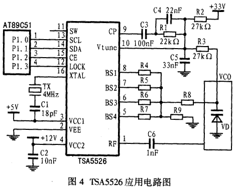
Refgadj: CLR P1.0
SETB P1.2
MV R0, # 08H
Frigadj1: MOVA A, 20H
CLR C
RRC A
MOV P1.1, C
SETB P1.0
NOP
CLR P1.0
DJNZ R0, Frigadj1
MOV R0? # 08H
Frigadj2: MV A, 21H
CLR C
RRC A
MOV P1.1, C
SETB P1.0
NOP
CLR P1.0
DJNZ R0, Frigadj 2
MV R0, # 08H
Frigadj 3: MOVA A, 22H
CLR C
RRC A
MOV P1.1, C
SETB P1.0
NOP
CLR P1.0
DJNZ R0, Frigadj 3
MV R0, # 03H
Frigadj 4: MV A, 23H
CLR C
RRC A
MOV P1.1, C
SETB P1.0
NOP
CLR P1.0
DJNZ R0, Frigadj 4
RET
Neckband Earphones,Neck Earphones,Best Neckband Earphones,Wireless Neckband Earphones
Dongguang Vowsound Electronics Co., Ltd. , https://www.vowsound.com