The digital signal processor DSP is a microprocessor with a special structure, which is specially designed for implementing various algorithms of digital signal processing, and thus has a special hardware structure. The TS201 is a high-speed DSP that integrates fixed-point and floating-point calculations in the TIGERSHARC family of Analog Devices. The processor is widely used in the video, communication market and defense military equipment, and is suitable for applications with large data volume real-time processing.
The TIgerSHARC series DSP bootloader is very flexible and can be flexibly selected according to the needs of the actual system. A radar signal processor adopts a 6U shape, and the CPCI bus adopts the European card size standard, and performs data communication with the host through the CPCI bus. Aiming at the hardware system of the signal processor, this paper proposes a booting scheme, which uses the CPCI bus to transmit the boot code to the board, and then relies on the FPGA to boot the DSP from the link port.
1 ADSP-TS201 boot mode
The DSP boot is the process of loading the algorithm program code from the DSP external memory in the case of a DSP system reset. The TS201 supports two boot modes: Master Boot mode and Slave mode.
In the main boot mode, the TS201 acts as the active party, using the external port to output the address, and the read boot mode is selected ( ![]() ) and other control signals to load code from EPROM or FLASH. In the slave mode, the TS201 acts as a passive party and does not output control signals to the outside. The external host or other device transmits the code to be loaded to the host or link port of the TS201. The TS201 only starts several DMA channels and executes the first DMA. The loaded core is received.
) and other control signals to load code from EPROM or FLASH. In the slave mode, the TS201 acts as a passive party and does not output control signals to the outside. The external host or other device transmits the code to be loaded to the host or link port of the TS201. The TS201 only starts several DMA channels and executes the first DMA. The loaded core is received.
In addition, FS201 can also choose a "non-boot" mode, or use TS201's (emulator) USB-ICE loader, this method can directly load the program into the internal RAM of TS201 or external RAM, DSP directly from The program is run in RAM and is often used in the debugging process of the DSP.
Through the TS201 ![]() The setting of the pin can set the boot process of the DSP to the master boot mode or the slave boot mode. During the DSP reset, if the pin is low, the main boot mode is selected, and the DSP loads the program from the external EPROM or FLASH;
The setting of the pin can set the boot process of the DSP to the master boot mode or the slave boot mode. During the DSP reset, if the pin is low, the main boot mode is selected, and the DSP loads the program from the external EPROM or FLASH; ![]() When the pin is high, it enters the slave boot mode, the DSP is idle, and waits for the host or link port to load the program. Both boot modes have the same loading process, as follows:
When the pin is high, it enters the slave boot mode, the DSP is idle, and waits for the host or link port to load the program. Both boot modes have the same loading process, as follows:
(1) The TS201 automatically starts a DMA and automatically transfers 256 words (32 bits) to the internal memory address 0x00 to 0xFF.
(2) The TS 201 executes the above 256-word instruction (load core), loads the core to start other DMA, and loads subsequent instructions and data into the internal and/or external memory.
(3) Load the core self-coverage and execute the DSP algorithm program.
The booting scheme of the system adopts the slave boot mode, transfers the code from the host to the FPGA through the CPCI bus, and then starts the DSP through the link port by using the FPGA.
2 Guide design of a radar signal processor
Based on a radar signal processor hardware processing platform, a multi-DSP boot design scheme as shown in Figure 1 is employed.
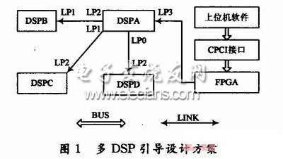
The algorithm code (.LDR file) of the four DSPs is transmitted to the FPGA through the host computer software, and the FPGA loads the program to the DSPA through the link port with the DSPA. After the DSPA is successfully loaded, the DSPB, DSPC, and DSPD are booted separately.
The advantage of loading DSP in this way: When debugging DSP, you can not use JTAG emulator; at the same time, when DSP starts, you can use FLASH or E2PROM to store program code. There is no limit to the size of DSP program, and it also saves board. Space and its hardware design complexity.
The difficulty of loading DSP in this way: CPCI bus and FPGA data transmission error and FPGA and TS201 link port communication, these two difficulties have been solved in the actual project. The CPCI bus and FPGA interface can use PLX9656 chip to complete data transmission, so the design of this loading mode is feasible.
2.1 automatic boot program design ideas
In order to design a load (auto-boot) program, you must first understand the software design flow of the ADSP-TS201. The flow chart is shown in Figure 2.
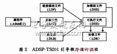
Among them, the link description file (.LDF) defines the memory configuration of the entire system and the specific storage location of the data and code in the program. The load kernel file (.DEX) refers to the load boot kernel program. Its function is to synthesize the executable file (.DXE) compiled by the user project into a link port loading mode output file (.LDR). This load output file is used to define how the internal and external memory of the TS201 is initialized during loading.
In the ldr subdirectory of the VisualDSP++ installation directory, Analog Devices provides standard loading kernel files and corresponding source programs (.ASM) and linker script files. Generally, the standard load core file provided or the corresponding source program can be directly modified to recompile the load core file generated by the link. The load file is changed by the boot loader (elfloader) to a certain format of the executable file, and the load kernel file is added at the starting position.
Since the TS201 has three boot modes (regardless of the non-boot mode), Analog Devices offers three different loads and files, which are divided into: TS201_prom.dxe, TS201_li-nk.dxe, TS201_host.dxe. The core ideas and functions of the three programs are exactly the same, but there are slight differences in the implementation of the specific code due to the different loading ports and methods used. Because the system uses the link port to start, and the DSPA, DSPB, DSPC, and DSPD are all started with different link ports, the link file is used to load the core file, and the loaded core file needs to be modified slightly to meet the link-free interface. Startup requirements.
2.2 This signal processor reset guide design flow
As shown in Figure 1, the program to be run by the four DSPs is finally read by the host computer and transmitted to the FPGA through the CPCI bus. The four DSPs are in the link port boot mode. After the DSP is reset, the DSPA loads the program from the FPGA. After the DSPA is loaded, it loads the DSPB, DSPC, and DSPD through the link port. After the loading is completed, the four DSPs execute their respective programs normally.
Combined with the analysis of the above parts, it can be seen that to achieve the correct guidance of the four DSPs in the signal processor, the required work consists of the following steps:
(1) The program to be executed by the DSPB (DSPB.dxe) is combined with the load core program of the link port to generate the DSPB load file (DSPB_bin.ldr). It should be noted that the link port loading core program cannot directly use the provided standard link port loader. You must change the LINK constant in the provided link port loading core file (TS201_link.asm) to 1 (#define LINK). 1), that is, DSPB is guided by link port 1.
(2) Similar to (1), generate the DSPC load file (DSPC_bin.ldr), but only need to change the LINK constant in the link port loading core file (TS201_link.asm) to 2 (#define LINK 2), ie DSPC Booted by link port 2. Similarly, the DSPD is loaded by link port 2, and the DSPD load file (DSPD_bin.ldr) is also generated.
(3) Since the DSPA wants to program the DSPB, DSPC, and DSPD through the link port, it is necessary to add the boot program of all the ADSPTS2 01 at the beginning of the program when programming the DSPA. The program of each ADSP-TS201 is composed of the boot code and the user program, so the data of the complete .1dr file will be transmitted when the DSPA transmits the program to the rest of the DSP.
Generally speaking, LED Video Processor, is the LED display screen dedicated video processor.And the the task, in simple terms, is to change the image signal from other accessaries (such as DVD, computer, Camera, hd broadcast box, etc.) to the data that LED display would be accept.
Video processor is the witness of full color LED display screen in the whole process of the birth, growth, maturity and iconic device. LED dedicated video processing equipment in the process also gradually mature, LED video processor quality directly affect the effect of the LED display.

Video Processor
Video Processor,Led Display Video Processor,Led Display Accessory,Led Display Controller
Shenzhen Priva Tech Co., Ltd. , https://www.privaled.com