Introduction
Autoclave testing, also known as autoclave testing, is a quality test that is typically required for devices used in harsh environments. Until recently, the automotive safety industry began to propose autoclave test requirements to test MEMS accelerometers for airbag sensors [1]. For this test, the device was stored in an environmental test chamber without charge for 96/168 hours, the ambient test chamber had a gas pressure of 15 psig, a temperature of 120 °C, and a relative humidity of 100%. After a certain exposure time of the autoclave, the device was retested at room temperature.
Although the sensor's sensing structure is packaged in a sealed environment to prevent moisture intrusion, MEMS accelerometers are subject to autoclave pressure because plastic packaging materials absorb moisture under overpressure and under-wet conditions. To test the accelerometer's susceptibility to autoclave pressure, we placed 80 MEMS accelerometers under autoclave test conditions. As shown in Figure 1, the accelerometer consists of a MEMS sensing unit (g-cell) and a control ASIC assembled in a QFN package using a stacked chip structure. The sensing unit consists of a Freescale dimeric surface microflow that is sealed in a sealed cavity by wafer bonding techniques using a glass frit.
Autoclave test results show that at 25oC, 9 components cannot reach the offset specification, requiring 9-bit output offset variation of less than +/- 26 counts. The maximum offset change for a failed component is -48/+39 counts. When the part was tested for 168 hours, more device failures were found (same as the failure behavior of the offset change). These components were also found to have small offset variations and a tighter distribution at -40oC and 125oC. The failed device also shows a "self-healing" behavior of slow regression specifications after exposure to air for a period of time. The 120 ° C roasting under normal atmospheric conditions can accelerate the recovery process. The failure and recovery process is repeatable and reversible.
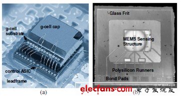
Figure 1. MEMS accelerometer: (a) QFN package view (mold cap not shown); (b) LSM angle sensor cell chip view
To determine the source of autoclave failure, we created a failure analysis fishbone diagram (Figure 2) to provide a comprehensive view of all possible causes of offset changes in autoclave test conditions (humidity, pressure, and temperature). Design and manufacturing processes were reviewed in four main areas: packaging, ASICs, sensors (g-cells), and testing. Therefore, three failure mechanisms unique to micromechanical sensing were discovered. These three mechanisms are:
Package stress resulting in offset variation Resistance leakage Parasitic capacitance change II. Package stress effectEpoxy resin encapsulated (EMC) materials absorb moisture and absorb heat to expand [2]. Scanning acoustic microscopy (C-SAM) inspection also revealed excessive delamination between the composite mold and the lead frame. These changes can change the stress state of the package and sensing unit, causing offset changes. FEA package modeling (Figure 3) is used to simulate the effects of this stress change. This model takes into account the asymmetric stratification between the EMC and the leadframe. Based on the principle that the water uptake is greater than 0.54% at equilibrium, the test also assumes a hygroscopic stress of 0.15%.

Figure 2. Autoclave failure analysis fishbone diagram
The FEA simulation results show that the inertial mass displacement of the sensor is quite symmetrical, but the displacement field of the package is asymmetrical due to delamination and hygroscopic expansion. The simulations show that the displacement caused by hygroscopic expansion is the same as the displacement caused by thermal strain at 125 °C. The maximum offset change caused by the package stress is predicted to be only 4 counts (worst case).
The main EMC portion around the sensing unit is removed by laser etching to further analyze the failed device. The idea behind this is that the stress field of the package will change dramatically, which can cause offset changes if the device is sensitive to package stress. However, the test results show that after most EMC removal, the device has only a very small offset change. This result is in line with the original FEA prediction, EMC's hygroscopic expansion will only have a very small impact on the offset change, and the package stress is excluded as the root cause of the autoclave failure.
Although studies have shown that package stress is not the source of autoclave failure, it is worth mentioning that this is due to stress-insensitive sensor/package design. The moisture absorption stress of the package is very large, and if the sensor is not designed correctly, it may become the main cause of failure of the autoclave. Design strategies to reduce the susceptibility to packaging stress have been discussed in [3].
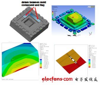
Figure 3. FEA simulation of EMC hygroscopic expansion
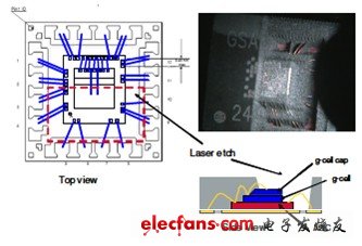
Figure 4. Stripping analysis to eliminate package stress as a source of failure
4-layer Medical Treatment PCB Board, Base Material: FR4 TG135. inner/outer copper thickness 1/1.5 oz. Immersion Gold 3U" surface finished. With green colour solder mask and white silkscreen. Board thickness 1.0 mm. Min.line width/Min.line spacing 0.12/0.15 mm. 20-up connect with the routed&v-cut, 100% E-test pass. there are Vias in pad need to be filled with resin and copper cap. Outline Profile tolerance +/-0.1 mm. line width / distance tolerance +/-15%. hole copper 30 um.The medical treatment PCB boards are usually of high precision, strict control of various tolerances required

Medical Treatment PCB Board,Medical Treatment PCB Panel,Medical Treatment Circuit Board,Circuit Board Etching
Orilind Limited Company , https://www.orilind.com