Introduction The multifunctional wireless mouse includes a wireless transmitting part and a wireless receiving part, where the transmitting part is a key part related to its overall performance. This system uses nRF24L01 as the core to build a wireless transmission module.
nRF24L01 is a new type of monolithic RF transceiver device, working in the 2.4 ~ 2.5 GHz ISM band; built-in frequency synthesizer, power amplifier, crystal oscillator, modulator and other functional modules, and integrated enhanced ShockBurst technology, The output power and communication channel can be configured through the program. nRF24L01 has low power consumption. When transmitting at 0 dBm, the operating current is only 11.3 mA; when receiving, the operating current is only 12.3 mA; multiple low-power operating modes (power-down mode and idle mode) enable energy-saving design more convenient.
The multi-function wireless mouse is a battery-powered handheld device, and power consumption is an important criterion to measure its performance. The main control chip selected for this design is MSP430F413, which is a 16-bit ultra-low power mixed signal processor. The maximum current in active mode is 350μA, and the power consumption in RAM data retention mode is only 0.1μA. The light sensor chip uses ADNS-5030. This chip is small in size and low in power consumption. In working mode, its maximum operating current is 17 mA; only when the optical sensor is working, the LED is lit, which will further reduce the power consumption of the optical sensor (less than 1 mA).
This article introduces the development process of the multi-function wireless mouse launching part, and discusses the precautions and optimization methods in its design and application. In the design process, paying more attention to details and optimization methods can make the design more smooth and provide effective time for large-scale algorithms.
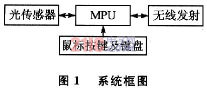
1 Hardware circuit design The transmitter part of the multi-function wireless mouse mainly realizes the collection of the displacement of the optical sensor and the key value, and transmits it to the receiver through wireless. It is mainly composed of control part, light sensor part, mouse button and keyboard part and wireless transmitting part. The system block diagram is shown in Figure 1.
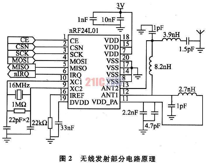
1.1 Wireless transmission part The wireless transmission part is the main part of the multifunctional wireless mouse. This design uses nRF24L01 as the core to build a wireless transmission module.
nRF24LOl has the unconditional use of the 2.4 GHz global open ISM frequency band, built-in hardware CRC error detection and one-to-multipoint communication address control, etc. The data transmission rate is 2 Mb / s, 126 channels; it can meet multipoint communication and frequency hopping The need for communication; low power consumption, the power supply voltage is 1.9 ~ 3.6 V, the operating current is 22 μA in standby mode, and only 900 nA in power-down mode. These are the main advantages of nRF24L01.
The circuit principle of the wireless transmitting part is shown in Figure 2.
 1.2 Power management Hand-held systems have strict requirements for low power consumption. There are 5 low power consumption modes of MSP430 series single chip. When there is no operation for a certain period of time, it can be put into a certain low power consumption mode, and the working current at this time can be controlled below a dozen μA.
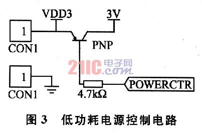
For peripheral devices, such as light sensors and wireless transmitters, a switch is set to cut off their power before the main control chip enters a low-power mode, so that the system's power consumption is further reduced. When an operation arrives, the main control chip returns from the low-power mode to the active mode, first turning on the power switch of the peripheral device, so as to ensure the normal operation of the system. The low-power power supply control circuit is shown in Figure 3. The switch consists of a PNP-type transistor, the base is used as the input of the control signal, the emitter is the voltage input, and the collector is the voltage output. The level change of the control signal can control the power on and off on the line.
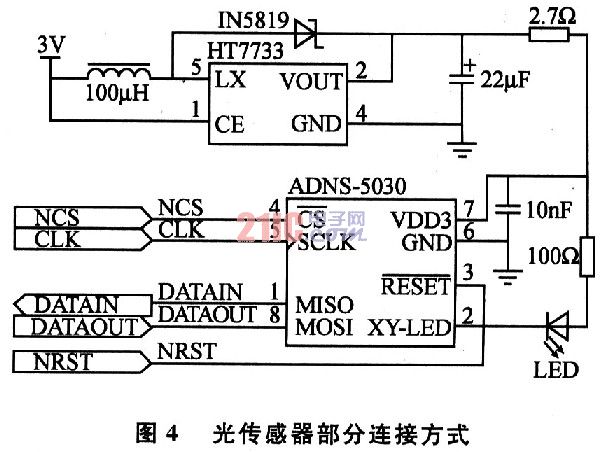
1.3 Light sensor part The light sensor ADNS-5030 is used for mouse positioning. The normal working voltage of ADNS-5030 is 3.3 V. In the design of the light sensor, it is necessary to output the battery power. The OV voltage is converted to the required 3.3 V voltage. The circuit uses HT7733 chip to complete the voltage conversion. ADNS-5030 performs data communication with the main control chip through the SPI bus, and its connection mode is shown in Figure 4.
1.4 Buttons and keyboard The buttons of the multi-function wireless mouse are basically the same as those of the ordinary mouse, except that the wheel of the ordinary mouse is changed to the design of the up and down keys. The functions of these two designs are the same. The keyboard is used to input Arabic numerals, letters and various function keys. The matrix type mobile phone keyboard is used, which saves the I / O port resources of the main control chip.
2 Software design
2.1 General I / O simulation SPl interface The wireless transmitter chip nRF24L01 and the light sensor ADNS-5030 are all used SPI bus to exchange data with the main control chip. For cost considerations, the main control chip MSP430F413 selected in this design does not have an SPI bus interface. Therefore, a general-purpose I / O port is required to simulate the SPI interface.
To simulate the SPI serial interface with the general-purpose I / O port, the bus timing of the device SPI must be strictly observed. ADNS-5030's SPI bus timing has several points to note: First, the serial clock frequency of the SPI bus should be less than 1 MHz. If the clock frequency of the SPI bus is too high, the device cannot respond in a short time, and the corresponding operation It cannot be completed; Second, ADNS-5030 requires a 50% duty cycle for the clock signal on the SPI bus. This requirement is not for all devices, but for specific examples of such requirements, it must be followed. (Experiment proves that this conclusion is correct. The author fills the vacancy by adding a blank instruction in the program to make its duty cycle meet the requirements of the device); Third, there are many necessary delays in SPI bus operation, such as read operation There is a delay of 4 μs between the write address and the read data. Without this delay in the program, normal read and write operations cannot be performed.
2.2 The wireless transmission part The working principle of nRF24L01 is as follows: When transmitting data, first configure nRF24L01 as the transmission mode, and then write the receiving node address TX_ADDR and valid data TX_PLD into the nRF24L01 buffer area by SPI port according to the timing. TX_PLD must be written continuously when CSN is low, and TX_ADDR can be written once during transmission. Then, the CE is set to a high level and held for at least 10 μs, and data is transmitted after a delay of 130 μs. If the automatic response is turned on, then nRF24L01 enters the receiving mode immediately after transmitting data, and receives the response signal (the automatic response receiving address should be consistent with the receiving node address TX_ADDR). If a response is received, the communication is considered successful, TX_DS is set high, and TX_PLD is cleared from TX_FIFO; if no response is received, the data is automatically retransmitted (automatic retransmission is on), if the number of retransmissions (ARC) When the upper limit is reached, MAX_RT is set high, and the data in the TXFIFO is reserved for retransmission. When MAX_RT or TX_DS is set high, IRQ becomes low, an interrupt is generated, and the MCU is notified. When the transmission is successful, if CE is low, nRF24L01 enters standby mode 1; if there is data in the sending stack and CE is high, then enter the next transmission; if there is no data in the sending stack and CE is high, then enter standby mode 2.
When receiving data, first configure nRF24L01 to receive mode, and then delay 130μs to enter the receiving state to wait for the arrival of data. When the receiver detects a valid address and CRC, the data packet is stored in the RXFIFO, and the interrupt flag bit RX_DR is set high, IRQ becomes low, an interrupt is generated, and the MCU is notified to fetch the data. If the automatic answer is turned on at this time, the receiver enters the transmitting state and returns the answer signal at the same time. When the reception is successful, if the CE goes low, the nRF24L01 enters standby mode 1.
nRF24L01 has 4 working modes: transmit, receive, standby and power-down, its working state can be set through configuration register, as listed in Table 1.
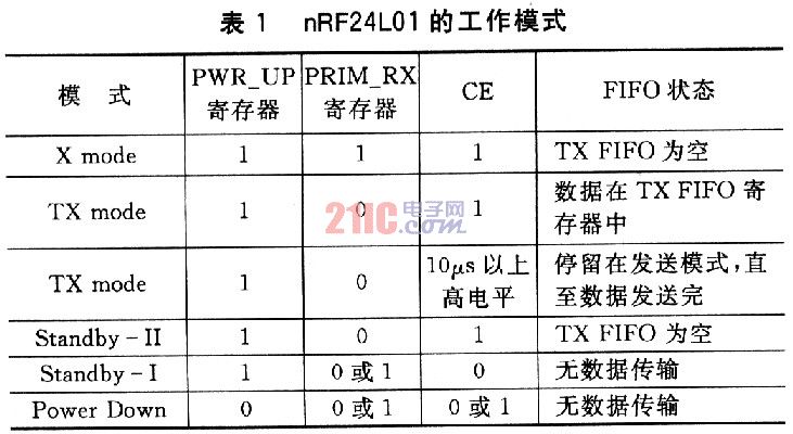 Standby mode 1 (Standby-I) is mainly used to reduce current consumption (in this mode, the crystal oscillator is still working). Standby mode 2 (Standby-II) is to enter this mode when the FIFO register is empty and CE = 1. In standby mode, all configuration words remain. In Power Down mode, the current consumption is minimal, and the nRF24L01 also does not work, but the values ​​of all its configuration registers are still retained.
When the wireless transmitter is powered on and initialized, the following configuration is performed:
â‘ The lower 4 bits of the CONFIG register are 1, respectively, 16-bit CRC check, chip power-on and receiving mode;
â‘¡SETUP_AW (address width) register configuration address width is 5 bytes;
③SETUP_RETR (automatic retransmission) register is configured for automatic retransmission delay 500μs, retransmission 5 times;
â‘£ The RF_CH (RF channel) register is configured as the working channel 2400MHz;
⑤ The RF_SETUP (RF setting) register is configured to transmit power O dBm, Air Data Rate is 1 MHz;
â‘¥Write the address to the address register.
One thing to note when configuring the register: When writing the nRF24L01 register, it must work in power-down mode or standby mode. And the nRF24L01 power up to l. After 9 V, a power-on reset of 10.3 ms is required before entering power-down mode. This is an uncertain state. In this state, the write operation to the register cannot be completed, so an appropriate delay must be added to allow the program to configure the nRF24L01 in power-down mode or standby mode.
When the light sensor or keys are operated, the main controller writes the read signal into the TX_PLD of nRF24L01, and then the chip automatically generates the header and CRC check code and sends it out. When the response signal (ACK) is received, the flag bit success set in the program is set to 1, the data in the TX FIFO queue is cleared, and the next data can be written; if the response signal (ACK) is not received, then The success bit is set to 0, and retransmission continues, and new data cannot be written.
2.3 Reading the displacement value of the light sensor Reading the displacement value of the light sensor is actually reading its corresponding register. In the internal register of ADNS-5030, the MoTIon register at address Ox02 is used to indicate whether there is a displacement. If the highest bit is O, there is no displacement; if the highest bit is 1, there is displacement. In addition, the addresses of the two registers used are DeltaX and DeltaY of Ox03 and Ox04. The values ​​of these two registers represent the displacement in the X-axis and Y-axis directions, respectively. The highest bit indicates the direction of displacement, 1 is the negative direction, O is the positive direction, and the lower 7 bits indicate the amount of displacement.

As shown in Figure 5, first determine whether there is a shift, that is, whether the highest bit of MoTIon is 1. If it is not 1, it means there is no displacement, and the query ends; if it is 1, it means there is displacement, and then read the values ​​of DeltaX and DeltaY, and send them out through the wireless transmission part.
After reading the DeltaX and DeltaY registers, the value in the register is automatically cleared, but the MoTIon register is not cleared after reading, so the last bit of the MoTIon register needs to be cleared to prevent the system from performing DeltaX , DeltaY register scanning, causing unnecessary waste.
Another point to consider is the resolution of the light sensor. After power-on reset, the resolution of the light sensor is the default 500 cpi (cells perinch), but the experimental effect is not good. During debugging, its displacement is not obvious. Later, the value of the register was modified, and its resolution was changed to 1 000 cpi (only two resolutions of 500 cpi and 1 000 cpi). The displacement effect of the cursor is significantly better than the resolution, The effect at 500 cpi. This shows that this property of the light sensor is also very important.
2.4 Reading keys and keyboard The design of the left and right keys is slightly different from the design of ordinary keys. When using the mouse, you can see that when you drag the mouse while pressing the left button, you can select the options within the cursor movement range; similarly, the right button also has such a function.
In the left and right key scanning program, when the program scans that a key is pressed (for example, the left key is pressed), the obtained key value is immediately sent out. At this time, the left key value of the receiving end is always in the pressed state At the same time, it does not delay the scanning of the light sensor, etc .; when the left button is lifted, it sends the button lift instruction to the receiving end, and the scan of the left and right buttons is completed. In this way, when the left button is pressed and the mouse is dragged at the same time, the operation of selecting the options in the cursor movement range is selected.
The up and down keys operate differently from the left and right keys. In the scanning procedure of the up and down keys, two different situations of jog and linkage should also be considered. Jog is to press a key quickly within a certain time and then release it immediately; and press a key and release it after a delay, the program will recognize it as a linkage.
The keyboard part is set with 20 keys, which is a 5 × 4 matrix, including “O ~ 9†10 numeric keys, “up, down, left, right†4 direction keys, “â†â€ key, “OK†key , "Esc" key and 3 shortcut keys ("Show Desktop", "Browser" and "My Computer"). Among them, the ten numeric keys from "0 to 9" are multiplexed keys. Like the keyboard of a mobile phone, different key values ​​can be input according to the number of consecutive taps in a certain period of time.
Conclusion The hardware involved in this article was debugged in practice. Experiments prove that the MSP430 series MCUs have lower cost and are widely used in low-power products, and will be recognized by the majority of developers. This system has realized the basic functions of combining mouse and mobile phone keyboard, and its functions can still be supplemented in the future to improve the performance of multi-function wireless mouse.
Fahold, a 8 year old company brings light power to your life by illuminating your offices, factories, warehouses, shopping malls, airports, etc. with its high quality LED Troffer lighting products and solutions.With global manufacturing standards and various certifications including CE,TUV, UL and FCC, our lighting products are sold in domestic market and are exported to various international markets including US, UK, France, Germany, Australia, Africa, Korea etc. We offer a wide range of Lighting source for Led Lighting Solutions which includes LED TrofferLighting or System, , LED Lams, LED Panel etc. At the same time Maximize beauty of your workplace with our powerful driver to drive Warehouse Lighting, Workshop Lighting, Supermarket Lighting and Factory lighting solutions. We have skilled engineers to answer all your questions and enquiries and provide all-round solutions basis on your project(s) and provide technical supporting.
Application: Specifically for led Troffer light,AC100-277V/347V,1-1.5A output current,Iron box casing, support 0-10V/PWM/RX dimming, High efficiency and PF value, Pass the UL/FCC/Class P certified for North America market.
Parameter:
Input voltage:100-277V
Output voltage:25-40V
Current:1100mA/1500mA
PF:>0.9
THD:<15%
Size style: Iron box, long slimline.
Dimming:0-10V / PWM / RX / DALI.
>=50000hours, 3-5 years warranty.

What's the benefits of Fahold led Troffer lights driver?
- Standard Linear Lighting
- Cost-effective light-line solution for industry,commercial and other applications
- Good quality of light with high lumen output to meet different requirements
- Easy to order and install,requiring less time,reducing packaging waste and complexity
- Flexible solution
FAQ:
Question 1:Are you a factory or a trading company?
Answer: We are a factory.
Question 2: Payment term?
Answer: 30% TT deposit + 70% TT before shipment,50% TT deposit + 50% LC balance, Flexible payment
can be negotiated.
Question 3: What's the main business of Fahold?
Answer: Fahold focused on LED controllers and dimmers from 2010. We have 28 engineers who dedicated themselves to researching and developing LED controlling and dimming system.
Question 4: What Fahold will do if we have problems after receiving your products?
Answer: Our products have been strictly inspected before shipping. Once you receive the products you are not satisfied, please feel free to contact us in time, we will do our best to solve any of your problems with our good after-sale service.
LED Troffer Driver
600X600 Panel Light Driver,5Years Warranty Driver,Junction Box Driver
ShenZhen Fahold Electronic Limited , https://www.fahold.com