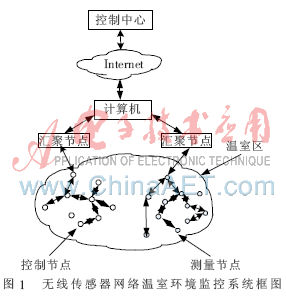
The overall structure block diagram of the greenhouse environment monitoring system is shown in Figure 1. The sensor measurement nodes and control nodes with simple execution control functions are used in the network to form a wireless sensor network. The measurement node is used to measure important environmental data such as air temperature, humidity, light intensity, etc. The control node (which can control the temperature and humidity control equipment) is used to receive the remote control information from the computer in order to properly adjust the greenhouse environmental parameters Regulation. The data collected by the measurement node is transmitted along the other measurement nodes in a multi-hop manner. During the transmission process, the monitoring data may be processed by multiple measurement nodes. The information arrives at the sink node after the multi-hop route, and the sink node will directly receive the received data. Uploaded to the computer, all data is processed by the computer for complex digital signal processing, and the sensor network is configured and managed through the database, monitoring tasks are released and information such as monitoring data is collected. Finally, these data can also interact with the remote control center through the Internet To achieve remote monitoring of the greenhouse environment.
2 Introduction to CC2431 CC2431 is a product of TI. It is a true system-on-chip based on wireless sensor network ZigBee / IEEE802.15.4 solution. It integrates CC2420 RF transceiver, industry standard enhanced 8051 MCU core, 128 KB Programming flash memory, 8 KB of RAM, precise positioning engine and other rich on-chip resources, support hardware debugging, support online debugging based on IAR7.20 and above C51 development environment, provide powerful and flexible development tools. CC2431 is small in size, low in power consumption and high in integration, which is very suitable for the design of wireless sensor network nodes. It can work in 4 working modes, and the conversion time between the working modes is short, so it can meet the requirements of ultra-low power system design.
3 Hardware of the sensor network node The sensor network node is composed of a sensor measurement node, a control node and a convergence node. The measurement node is responsible for collecting the surrounding environment information. The collected environment information reaches the convergence node after multi-hop routing, and finally reaches the control center through the Internet. The control node is used to receive the remote control information from the computer and adjust the greenhouse environment parameters.
3.1 Measurement node hardware The sensor measurement node consists of a sensor module, a microprocessor module, a wireless communication module and a power module. The block diagram of its hardware structure is shown in Figure 2.

(1) Sensor module. It is composed of different types of sensor chips and has the ability to perceive temperature, humidity and light intensity. Among them, the temperature and humidity sensor uses the I2C bus digital temperature and humidity sensor SHT11, which has a small size, low energy consumption, a two-wire digital interface, a temperature range of -40 ° C to 85 ° C, and a relative humidity range of 0% to 100% RH. The light intensity sensor uses TSL2550D, its power consumption can meet the requirements of wireless sensor low power system design, and its bus is also easy to interface with CC2431.
(2) Microprocessor module. Using 8051 CPU integrated inside CC2431. The integrated CPU has 4 different memory spaces: code area, data area, extended data area, and special function register area. Different memory spaces are conducive to the separation of code and data, and increase the speed of CPU access to memory.
(3) Wireless communication module â‘ Sensor network nodes consume a lot of energy during communication. Selecting a low-power wireless communication chip will effectively reduce the energy consumption of the communication module. CC2431 is a low-power communication chip that complies with the ZigBee standard. It has the functions of fast wake-up and search for external devices. It can make the nodes sleep more and save power, and its parameters such as channel frequency and power consumption can be flexibly set. The antenna of the CC2431 communication module takes into account the requirements of wireless sensor network communication quality, and uses a unipolar antenna. The unipolar antenna requires the use of a "balance-unbalance transformer" between the differential output and the antenna.
â‘¡ The wireless sensor network node power supply is a battery-powered system, and the selected battery is a mobile phone dedicated lithium battery. In order to make the system work for a long time when the battery is powered, the energy saving of the node should be considered when designing the power module. CC2431 provides 4 power management modes: PM0, PM1, PM2, and PM3. Reasonably using these 4 modes can effectively reduce the energy consumption of the node.
â‘¢LED light is used to display the running status of the sensor node.
(4) Power module. Provide energy for other modules.
3.2 Control node The control node consists of driver module, microprocessor module, wireless communication module and power supply module. The driver module can perform related control on temperature adjustment, humidity adjustment and other equipment. Its hardware structure block diagram is shown in Figure 3.

3.3 Hardware Research of Convergence Node The convergence node is composed of a microprocessor module, a wireless communication module, a memory module, an Ethernet interface module, a serial interface module, and a power module. Its hardware structure is shown in Figure 4.

(1) The memory module consists of one AT45DB041 produced by Atmel, which is directly connected to the CC2431 SPI input terminal. The chip integrates 2 046 pages × 264 B Flash storage unit, used to store important historical data of the sensor.
(2) In order to provide an Ethernet access channel, in this design, DM9161 is used as the Ethernet physical layer interface. DM9161 is a low-power, high-performance CMOS chip that supports 10 MB / s and 100 MB / s Ethernet transmission. It plays the role of encoding, decoding, input and output data, so that the aggregation node can be easily Connect to the Internet to facilitate remote control.
(3) The serial interface module consists of a low-power MAX3232 and a COM female port. CC2431 serial port is connected to MAX3232 for level conversion, and communicates with computer through COM port.
(4) Because the aggregation node needs to fuse and process the data collected by all the collection nodes, and the data needs to be transmitted to the computer over a long distance, so the energy consumption is large, so its power supply adopts the method of intervening after conversion from the mains.
(5) The LED light is used to display the running status of the convergence node.
4 Transplantation of TInyOS operating system The embedded operating system can simplify the development of the embedded system, ensure the stability and reliability of the program operation, and facilitate the maintenance and update of the program, but because the wireless sensor network node is a small embedded system, its hardware The resources are very limited, and it is necessary to efficiently use its limited memory, processors and communication modules, and to minimize system energy consumption and extend the service life of the nodes. Therefore, the traditional embedded operating system cannot meet its requirements. Based on this, this article transplants the operating system TInyOS developed for the characteristics of wireless sensor networks.
4.1 Introduction to TInyOS TinyOS is a typical wireless sensor network operating system developed by the University of California, Berkeley. TinyOS-based applications can be developed through nesC language. The goals of TinyOS design are small code size, low energy consumption, high concurrency, and good robustness. It can adapt to different applications, adopt lightweight threading technology, event-driven mode, component programming, etc., making it wireless-oriented The operating system of the sensor network. TinyOS provides Main accessories, as well as perception components, execution components, communication components, and hardware abstraction components for certain hardware. On the basis of these components, users can customize and develop application components, and then connect all components to form the entire application.
4.2 Migration of TinyOS There are many versions of the TinyOS operating system. The version of TinyOS 2.0 to be transplanted is Keil. TinyOS 2.0 must work under the Linux platform, and Keil is a software under Windows. Therefore, install a software that simulates the Linux development environment running on the Windows platform-Cygwin. The following describes the transplantation steps:
(1) Install SmartRF04 Flash Programmer, Keil, Java 1.5 JDK, Cygwin software;
(2) Download the installation package of the necessary compilation tools for TinyOS development;
(3) Start Cygwin and install the downloaded compilation tool installation package under Cygwin;
(4) Install TinyOS 2.0.
Unzip the downloaded TinyOS 2.0 installation package, and copy the decompressed tinyos-2.0-contrib folder to the Cygwin \ opt directory. At this point, the TinyOS development environment has been set up. All examples are under tinyos-2.0-contrib / diku / common / apps /. Take BlinkNoTimerTask as an example, enter the following in Cygwin: cd / diku / common / apps / BlinkNoTimerTask, and then press Enter: make cc2431em, if it is successful, TinyOS will be compiled to generate an app.hex file, as long as this file is burned into the microcontroller That's it.
(5) Burn and insert the emulator, open the SmartRF04 Flash Programmer software, select the app.hex file under the System-on-Chip tab, and then select "Perform actions" to burn in sequence. After successful writing, TinyOS It was successfully transplanted to CC2431.
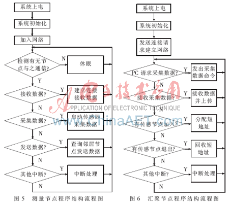
5 Software design of the sensor network node The main function of the sensor measurement node is to receive PC data collection instructions, collect data, and then send the collected data through a wireless channel. The function of the aggregation node is to create a wireless network, configure the network node attributes, receive the data collected by the sensor measurement node, and then upload it to the computer through the serial port. The flow chart of the sensor measurement node program structure is shown in Figure 5, and the flow chart of the aggregation node program is shown in Figure 6.
In agricultural production, with the emergence of large-scale operations, many greenhouses may be built. According to the design of the application, a wireless sensor network is built in each greenhouse. Since the environment in the greenhouse is relatively similar, therefore, The function and technology of the wireless sensor network in each greenhouse are also the same. If all greenhouses are managed by the computer of the control center, it can greatly improve the work efficiency, make the greenhouse management more scientific, and make the control simpler, so as to achieve the ultimate goal of improving crop yield, improving quality, regulating growth cycle, and improving economic benefits. . The wireless sensor network node introduced in this paper has the advantages of low power consumption, small size, reliable operation and easy expansion. The greenhouse environment monitoring scheme based on this wireless sensor network will have good application prospects.
FTTH Fiber Optic Splice Tray is designed to provide a place to store the fiber cables and splices and prevent them from becoming damaged or being misplaced. It is also called a splice enclosure or splice organizer. This device does not contain any technical functions, and the design is simple. Also, Fiber Optic Tray has a very low price for people to afford. However, the importance of fiber splice tray for protecting fibers is significant. And the skills needed for using a fiber splice tray is not as simple as you think.
Made by industrial high-quality ABS plastic, Fiber Optic Cable Tray is provided to place the fiber splice points and pre-terminated for fiber connectivity. The splice tray expands fiber splice capabilities as well as provides the splicing location for fiber optic cables. It can be put into the fiber distribution frame, fiber splice closure, optic terminal box, etc. Sijee offers different shapes of fiber splice tray with or without termination function. Fiber Optic Tray, Fusion Splice Box, Fiber Optic Cable Tray, Splice Tray Optic Fiber are available.
Applications:
Fiber splice trays are usually placed in the middle of a route where cables are required to be joined or at the termination and patch panel points at the end of the cable runs. Also, splices can be placed in a splice tray which is then placed inside a splice closure for OSP (outside plant) installations or a patch panel box for premises applications. As for indoor application, fiber splice trays are often integrated into patch panels to provide for connections to the fibers.


FTTH Fiber Optic Splice Tray
Fiber Optic Tray,Fusion Splice Box,Fiber Optic Cable Tray,Splice Tray Optic Fiber
Sijee Optical Communication Technology Co.,Ltd , https://www.sijee-optical.com