In this paper, an analog divider is designed. Based on the analysis and discussion of its working principle, the CSMC0.5um CMOS process is used to simulate the Cadence Spectre. The simulation results verify the theoretical analysis.
1 circuit design and analysis
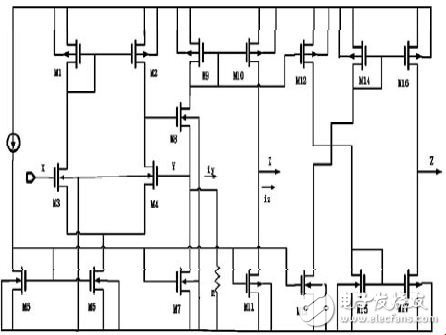
Figure 1 CCII circuit structure
The analog divider is powered by a single supply +5V and consists of two parts. The first part is the second generation current transmitter CCII, and Figure 1 is the CMOS CII circuit. Transistors M3 and M4 form a differential amplifier. The output of the amplifier is transmitted to the Y terminal through transistor M8, and the current mirror formed by transistors M1 and M2 is the active load of the differential amplifier. Assuming that transistors M1 and M2, M3 and M4, M9 and M10 are matched, transistors M5, M6, M7 and M11 form a bias current mirror that provides bias current for each of the three branches, and I7 = I11. The current mirror composed of transistors M1 and M2 forces the drain and source currents of transistors M3 and M4 to be equal, so that Vgs3=Vgs4, and transistors M3 and M4 are source-coupled pairs, so the gate voltages of transistors M3 and M4 are equal, that is, Vx=Vy. . Transistor M8 acts as a source follower and provides a low output impedance at the Y terminal. If Vy "0" and R is the Y-terminal resistance, the current flowing from the Y terminal is iy=Vy/R, and the drain current of the transistor M8 is (I7+iy), which is reproduced by the action of the current mirrors M9 and M10. To the Z end. Since I11=I7, the current flowing out of the Z terminal is equal to the current at the Y terminal, that is, iz=iy.
Transistors M12-M17 form a cross-coupled current mirror that replicates the current (I7+iy) to the Z port. Since current I16 follows current I7, current iz flows in the opposite direction, ie iz=-iy.
Thus, it can be seen that the CCII circuit can be implemented:
The second part of the voltage-current conversion circuit is shown in Figure 2. Transistors M20, M21 provide a constant and equal current source. Transistors M22-M25 operate in the saturation region and M26-M29 operate in the linear region. Ignore the body effect, the leakage current Id:
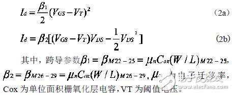
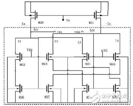
Figure 2 voltage and current conversion circuit
The circuit in the dotted line in Fig. 2 can be divided into four branches, which are composed of transistor pairs (M22, M26) (M23, M28) (M24, M29) (M25, M27). The voltages V1 and V2 are input signals. According to equations (2a) and (2b), we can get the relationship between current and voltage of four branches:
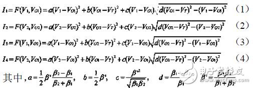
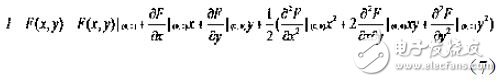
Equations (3)-(6) are expanded according to the Taylor series, and as shown in (7), they are expanded at the (0,0) point second order:
After integrating the path, the total differential output current is:
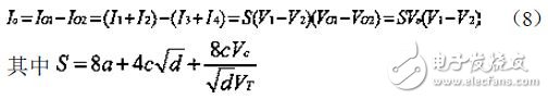
So, define the differential input V=V1-V2
And the differential input current:
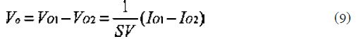
By equations (9), (10), (11), and (1)
Short Description:P2mm Indoor LED Module,256mmx128mm P2mm Indoor LED Panel with 128x64 pixels. Model:ERALED-P2-Indoor-128X64; 5 Years Warranty with NICHIA/CREE/NATIONSTAR/EPISTAR/SILAN gold wires LED lamps,1.6cm thickness PCB,MBI5153 Driving IC ;UL,CE,RoHS,FCC,3C,ISO Approved;
Fine pitch Indoor LED Module
256x128mm,128x64 pixels RGB full color SMD UHD P2mm Indoor Led Display Module |
||
|
Module Specifications |
||
|
1 |
Pixel Pitch |
2mm |
|
2 |
Pixel Configuration |
SMD3in1 |
|
3 |
Module Resolution |
128x64 pixels |
|
4 |
Module Pixles |
25,000 pixels |
|
5 |
Module Size |
256x128mm |
|
Specifications |
||
|
1 |
Screen Brightness |
≥1000cd/m2 |
|
2 |
Driving Method |
1/32 scan |
|
3 |
Mini Viewing Distance |
2m |
|
4 |
Max. Power Consumption |
750W/m2 |
|
5 |
Average Power Consumption |
320W/m2 |
|
6 |
Gray Level |
14bits input, 4096 levels(212) |
|
7 |
Display Color |
16M |
|
8 |
Frame Frequency |
≥60Hz |
|
9 |
Refresh Frequency |
≥1920Hz |
|
10 |
Uninterrupted Working Hours |
≥72 hours |
|
11 |
Screen Life-span |
≥100,000 hours |
|
12 |
MTBF |
≥5,000 hours |
|
13 |
Discrete Blind Spot Rate |
<1/10000 |
|
14 |
Continuous Blind Spot Rate |
None |
|
15 |
Blind Spot Rate |
<1/10000 |
|
16 |
Screen Plainness |
<±1mm |
|
17 |
Power Supply Mode |
AC220±10% 50Hz/AC110±10% 60Hz |
|
18 |
Environment Temperature & Humidity |
Temperature:-20 Celsius~+60 Celsius |
|
19 |
Control Mode |
Synchronous display with control PC by DVI |
|
20 |
Control System |
DVI video card + full color control card + fiber system( optional) |
|
21 |
Display Content |
Video, DVD, VCD, TV, picture, cartoon, graphics, texts.etc. |
|
22 |
Interface |
Standard Ethernet |
|
23 |
Transmission Distance |
Multi mode fiber <500m, single mode fiber <30km,internet cable <100m |

Fine pitch Indoor Led Module
High Power Led Module,Soft Flexible Led Display Screen,Pitch Led Display Screen,Curved Led Display Screen
Shenzhen Joy LED Display Co., Ltd. , https://www.joe-led.com