CB3LP chip introduction and internal block diagram
CB3LP chip is a kind of chip product successfully developed by Beijing Pan Analysis Intelligent Control Technology Co., Ltd. based on independent intellectual property rights research results "Sensorial Intelligence Control" (SIC). The product uses platform technology to improve the closed-loop automatic control performance of difficult-to-control objects, enabling engineers to design various fully intelligent fuzzy controllers quickly and easily.
CB3LP has intrinsic anti-jamming capability, and any fuzzy controller constructed with single-chip microcomputer can not be compared with it. For time-varying parameters and time-varying large-latency, difficult-to-control objects, the CB3LP control fluctuation is less than 0.2%; for easily-controlled objects, the CB3LP control fluctuation is less than 0.1 ‰. CB3LP externally connects a capacitor and two diodes and the internal circuit to construct an intelligent integral operation to achieve control without static errors; online automatic adjustment (embedded by single-chip microcomputer implementation) or offline manual adjustment of CB3LP external resistor to optimize the control response dynamic performance; CB3LP dynamic, Static control quality is better than fuzzy control; online (or offline) adjustment control performance is simple; strong anti-interference ability. Due to so many obvious technical advantages, its application range is very wide, and it is widely used in difficult-to-control objects such as high-precision control of time-varying parameters and time-varying large lag. It can also replace PID controllers for high-precision control of easy-to-control objects.
CB3LP is a functional fuzzy control chip, which integrates a functional fuzzy inference, that is, intuitionistic intelligent control function, an operational amplifier and a PWM generator, used to construct an intelligent controller. The control given input and feedback input of CB3LP are analog voltage signals; the control output is divided into analog and PWM two outputs, which can be selected by the customer; by changing the external circuit device, dual-mode control and intelligent integral operation can be added. See Figure 1 for its pin functions.
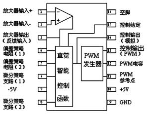
Figure 1 CB3LP internal functional block diagram
Design idea of ​​CB3LP chip in fluorescence quantitative PCR temperature control system The fluorescence quantitative PCR system is composed of basic PCR, fluorescence detection and host computer. Basic PCR is the basis of this instrument, including semiconductor cooling chips, temperature collection and processing, etc. It must have the basic requirements of PCR equipment such as precise temperature control, rapid temperature rise and fall, and uniform temperature to ensure the successful completion of the PCR process. The fluorescence detection part includes excitation light source, photomultiplier tube, signal acquisition and processing and other parts. The upper computer part includes data collection and system analysis software, which is mainly responsible for collecting data from the lower computer, forming real-time graphics, and performing data processing and graphic analysis to obtain the content of target DNA fragments and other test report information; at the same time, in the upper computer According to the PCR reaction conditions of the measured samples, set the corresponding temperature parameters, temperature control time and cycle number, etc., and then make the system enter the PCR cycle process of rapid temperature rise, constant temperature, rapid temperature decrease, constant temperature, etc., until all cycles are completed.
Figure 2 shows the block diagram of the CB3LP chip in the temperature control system. The host computer sends the given temperature signal to the single-chip microcomputer through the serial port, converts it to an analog signal through the DAC chip (AD667), and then amplifies it by the dual op amp LM358, and then adds it to the control given input terminal of the CB3LP chip; The platinum resistance is converted into a weak voltage signal. After being amplified by the three-op INA118 and the two-stage single op-amp 3140, it is divided into two outputs, one to the CB3LP chip and the other to the ADC chip AD574, which is converted into a digital signal and sent to the microcontroller and The set temperature is compared, and the single-chip microcomputer is controlled to output heating and cooling control signals. Finally, the PID control signal output from the optocoupler and the CB3LP chip is used to output the PID-adjusted heating and cooling control signals to the power reversing circuit of the semiconductor cooling chip to achieve accurate heating and cooling temperature control of the cooling chip.
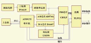
Figure 2 CB3LP chip in the temperature control system block diagram
The specific application design of CB3LP chip in temperature control system
1. Temperature measuring bridge and signal amplifying circuit The temperature measuring bridge and the signal amplifying circuit are shown in Figure 3. The temperature measuring bridge is composed of R5, R7, R8, R9, and PT1 platinum resistance, which converts the PT100 platinum resistance into a weak one. Voltage signal. PT100 has a resistance value of 100Ω at 0 ° C, and the resistance value increases by 0.385Ω for every degree of temperature increase. Under the condition of 0 ℃, make the resistance of PT1 100Ω, adjust R9, make the electric potential of B and D both ends of the bridge equal, then the bridge reaches equilibrium. When the outside temperature changes, the resistance of the sensor PT100 will change accordingly, the potentials at both ends of B and D are no longer equal, and the bridge is in an unbalanced state. There are load resistors R10 and R11 between B and D, and the output voltage is VBD. If R5, R7 and R8 are kept unchanged, then VBD will change when PT1 changes.
According to the functional relationship between PT1 and VBD, by detecting the unbalanced voltage VBD of the bridge, it can reflect the small change of the bridge arm resistance PT1. This is the basic principle of the work of the unbalanced bridge. In order to make the temperature measurement more accurate, instead of using the + 5V power supply of the external power supply, the voltage regulator TL431 is used, and its VOUT = (1 + R3 / R4) · Vref = 2 × 2.5V = 5V.
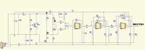
Figure 3 temperature measurement bridge and signal amplification circuit
The PT100 platinum resistance is transformed into a weak voltage signal, which is amplified by about 10 times by the three operational amplifier integrated circuit INA118. The internal block diagram of INA118 is shown in Figure 4. The magnification G = 1 + 50kΩ / R12 = 1 + 50 / 5.1 = 10.8. The voltage signal amplified by the three op amps is amplified by two 3140 single op amps and added to the input pin 1 of the same name of the amplifier of the CB3LP chip. It is also added to the 13 pin of the AD conversion chip U11 (AD574) and converted into a digital signal. Send to the single-chip 89C52, compare with the set temperature, control the single-chip P13, P14 to output heating and cooling control signals.
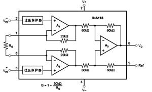
Figure 4 INA118 internal block diagram
The sensor uses a PT100 platinum resistance. Because the platinum resistance is measured by a small voltage, it is easy to be disturbed. Moreover, the platinum resistance is very small and it is easy to break down. Therefore, be careful when installing and try to stay away from the interference source. The signal amplifier circuit uses an op amp circuit. Carefully adjust the zero resistance of the op amp to zero the op amp.
2. Single-chip and its peripheral circuit Figure 5 is a single-chip and its peripheral circuit diagram, which is composed of ATMEL 89C52 single-chip system, AD and DA parts use 12bit conversion chip (AD chip AD574A, DA chip DA667) to improve the temperature control accuracy. AD574A is a single-chip high-speed 12-bit successive comparison A / D converter launched by American Analog Digital Corporation. It has a built-in bipolar circuit and a hybrid integrated conversion chip. It has the characteristics of few external components, low power consumption, high accuracy, etc., and has automatic Zero calibration and automatic polarity conversion function, only need to connect a small amount of resistance and capacitance parts to form a complete A / D converter. There are 12 data lines in AD574A. P0 of AT89C52 is directly connected with the upper 8-bit data line of AD574. The lower 4-bit data line of AD574A is directly connected with the upper half 4-bit P0.4 ~ P0.7 of the microcontroller. The fetch is based on the control line of the single-chip microcomputer for time-division gating. Pins 12 and 8 of the AD574A are data format selection terminals. When the level is high, the 12-bit data is valid at the same time; when the level is low, the first 8 bits are output, the second 4 bits are valid, and the high 4 bits are zero. This circuit is grounded at this foot and chooses to output 16bit data twice, of which 12bit data is what we need. The 4-pin A0 / SC of AD574A is a byte selection line. During conversion, when A0 is 0, AD574A performs 12-bit data conversion; when A0 is 1, AD574A performs 8-bit data conversion, and P2.3 is connected to A0. P2.2 connects to read conversion data control pin R / C, R / C is read / start signal, high level read data, low conversion. STS is the output terminal of the working state, the high level indicates that the conversion is in progress, and the low level indicates that the conversion is completed. Pin 13 of the AD574 is the input terminal of the measured voltage and receives the amplified signal from the temperature measuring circuit. Because an AD667 D / A conversion chip is also used, the CS terminal is controlled by the single-chip microcomputer and the converter is powered by a ± 12V power supply voltage.
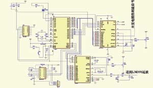
Figure 5 SCM and its peripheral circuit diagram
AD667 is also a single-chip high-speed 12-bit D / A converter launched by American Analog Digital Corporation. The control signal terminals are as follows: CS: D / A latch chip selection terminal (active low level), only when the CS terminal is an effective signal, Only then will the latch be activated. REFout: Reference output. REFin: Reference input. SPAN (10), SPAN (20): 10V, 20V range. SUM: summing end.
Digital input signal: DB0 ~ DB11 are digital input terminals, which are connected to the P0 port of the single-chip microcomputer. Like the AD574A, the data reading depends on the control line of the single-chip microcomputer to perform time-division gating. A0 ~ A3 is the address decoding input terminal, and the 9-pin Vout of AD667 is the analog output terminal. Its output voltage range can be selected by hardware programming, and unipolar and bipolar output can be realized. The analog signal output by this pin is amplified by the dual op amp LM358 (U5) and added to the control given input pin 15 of the CB3LP chip. The internal block diagram of AD667 is shown as in Fig. 6.

Figure 6 Internal block diagram of AD667
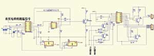
Figure 7 CB3LP chip control circuit
3. CB3LP chip control circuit Figure 7 shows the CB3LP chip control circuit diagram. The set target temperature value given by the host computer, PC, is sent to the single chip 89C52 through the serial port, converted into an analog signal by the DA conversion chip U12 (DA667), amplified by the dual op amp LM358 (U5), and then added to the control of the CB3LP chip. Fixed input pin 15; PWM control output pin 13 of CB3LP outputs a PWM signal, which is added to the optical coupler U6 (TLP521-4) through the Q2 shot stage 1, 3, and output from U6 16, 14; U6 The control signal output by the 16 terminal is added to the base stage of the transistor Q6, and the output is returned to the 12 terminal of U6 through the collector. The heating control signal output by P13 controls the conduction of the transistor Q3, controls the pin 5 of the optocoupler U6, that is, controls the conduction and end of the optocoupler U6 12, 11, and in the case of conduction, the signal controlled by the CB3LP chip passes 12, 11 of U6 give the heating signal adjusted by PID. The control signal output from the 14 end of the optocoupler U6 is applied to the base stage of the transistor Q5, and then output through the emitter back to the 10 end of the optocoupler U6. The cooling control signal output by P14 controls the conduction of the transistor Q4, and controls the 7-pin of the optocoupler U6, that is, the 10 and 9-pin of the optocoupler U6. In the case of conduction, the signal controlled by the CB3LP chip passes through the 10 and 9 pins of the optocoupler U6 to give a PID-regulated cooling signal.
Manually set addresses on the dmx lighting with the Iseeled Address Writer . The Led Address Writer is compatible with most professional lighting. The digital display of Dmx Writer allows for fast and easy setting addresses . ISEELED address writer is convenient for customers setting DMX addresses(such as DMX vertical tube, DMX flood light, DMX pixel lamp and so on)fast and easily. The addresses can be set by individually or uniformly with our address writer. Our address writer has the address setting function itself.
Photo show of Dmx Address Writer:


Dmx Address Writer,Address Writer,Led Address Writer,Dmx Writer
Shenzhen Iseeled Technology Co., Ltd. , https://www.iseeledlight.com