In the design of the PCB board, the anti-ESD design of the PCB can be realized by layering, proper layout and installation. ESD can be well protected by adjusting the PCB layout. When using a multi-layer PCB as much as possible, the ground plane and power plane, as well as the closely spaced signal line-ground spacing, can reduce common mode impedance and inductive coupling relative to a double-sided PCB, enabling it to reach 1/2 of a double-sided PCB. 10 to 1/100. It has components for the top and bottom surfaces and has a short connecting line.
Static electricity from inside the human body, the environment, and even electronic equipment can cause various damage to delicate semiconductor chips, such as penetrating a thin insulating layer inside the component; damaging the gates of MOSFETs and CMOS components; and flip-flops in CMOS devices Short-circuited, reverse-biased PN junction; short-circuited forward-biased PN junction; melted weld line or aluminum wire inside the active device. In order to eliminate the interference and destruction of electronic devices by electrostatic discharge (ESD), various technical means are needed to prevent them.
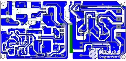
In the design of the PCB board, the anti-ESD design of the PCB can be realized by layering, proper layout and installation. In the design process, most of the design modifications can be limited to increasing or decreasing components through prediction. ESD can be well protected by adjusting the PCB layout. Here are some common precautions.
When using a multi-layer PCB as much as possible, the ground plane and power plane, as well as the closely spaced signal line-ground spacing, can reduce common mode impedance and inductive coupling relative to a double-sided PCB, enabling it to reach 1/2 of a double-sided PCB. 10 to 1/100. Try to keep each signal layer close to a power or ground plane. For high-density PCBs with components on the top and bottom surfaces, short traces, and many fill locations, consider using inner traces.
For double-sided PCBs, tightly interleaved power and ground grids are used. The power cord is placed close to the ground, and as much as possible between the vertical and horizontal lines or the fill area. The grid size on one side is less than or equal to 60 mm, and if possible, the grid size should be less than 13 mm.
Make sure every circuit is as compact as possible.
Keep all connectors aside as much as possible.
If possible, route the power cord from the center of the card away from areas that are susceptible to direct ESD.
Place a wide chassis ground or polygon fill on all PCB layers underneath the connector (which is easily hit directly by the ESD) and connect them with vias every 13mm.
A mounting hole is placed on the edge of the card, and the top and bottom pads of the solderless solder are attached to the chassis ground.
When assembling the PCB, do not apply any solder to the top or bottom pads. Use a screw with an inset washer to make the PCB in close contact with the metal chassis/shield or ground plane bracket.
The same "isolation zone" should be set between the chassis ground and circuit ground of each layer; if possible, keep the separation distance 0.64mm.
At the top and bottom of the card near the mounting hole, the chassis ground and the circuit ground are connected together by a 1.27 mm wide line every 100 mm along the chassis ground. Adjacent to these connection points, pads or mounting holes for mounting are placed between the chassis ground and the circuit ground. These ground connections can be made with a blade to keep open or jump with magnetic beads/high frequency capacitors.
If the board is not placed in a metal chassis or shield, solder resists should not be applied to the top and bottom chassis grounds of the board so they can act as discharge electrodes for ESD arcs.
To set a circular ground around the circuit in the following way:
(1) In addition to the edge connector and the chassis ground, a circular path is placed around the entire periphery.
(2) Ensure that the annular width of all layers is greater than 2.5 mm.
(3) Connect the ring shape with a via hole every 13mm.
(4) Connect the ring ground to the common ground of the multilayer circuit.
(5) For double panels installed in metal chassis or shielding devices, the ring ground should be connected to the circuit publicly. The unshielded double-sided circuit should be connected annularly to the chassis ground, and no solder resist should be applied to the annular ground so that the annular discharge can act as a discharge rod for the ESD, and at least one position on the annular ground (all layers) A 0.5mm wide gap prevents the formation of a large loop. The distance of the signal wiring from the annular ground cannot be less than 0.5 mm.
In the area that can be directly hit by the ESD, a ground line is placed near each signal line.
The I/O circuit should be as close as possible to the corresponding connector.
Circuits susceptible to ESD should be placed close to the center of the circuit so that other circuits can provide some shielding.
Place resistors and beads in series at the receiving end, and for those cable drivers that are easily hit by ESD, consider placing resistors or beads in series on the drive end.
A transient protector is usually placed at the receiving end. Connect to the chassis ground with short, thick wires (less than 5 times the width, preferably less than 3 times the width). The signal and ground wires coming out of the connector should be connected directly to the transient protector before they can be connected to other parts of the circuit.
A filter capacitor is placed at the connector or within 25 mm of the receiving circuit.
(1) Connect to the chassis ground or receive circuit ground with a short and thick wire (length less than 5 times width, preferably less than 3 times width).
(2) The signal line and the ground line are first connected to the capacitor and then connected to the receiving circuit.
Make sure the signal line is as short as possible.
When the length of the signal line is greater than 300mm, it is necessary to lay a ground wire in parallel.
Make sure that the loop area between the signal line and the corresponding loop is as small as possible. For every few centimeters of the long signal line, the position of the signal line and the ground line should be changed to reduce the loop area.
The signal is driven from a central location of the network into a plurality of receiving circuits.
Make sure that the loop area between the power supply and ground is as small as possible, placing a high frequency capacitor close to each power supply pin of the integrated circuit chip.
Place a high frequency bypass capacitor within 80mm of each connector.
Where possible, the unused areas are filled with ground and the fill areas of all layers are connected every 60 mm.
Make sure to connect to ground at two opposite end positions of any large ground fill area (approximately greater than 25mm & TImes; 6mm).
When the length of the opening on the power supply or ground plane exceeds 8 mm, connect the two sides of the opening with a narrow wire.
The reset line, interrupt signal line, or edge trigger signal line cannot be placed near the edge of the PCB.
Connect the mounting holes to the circuit ground or isolate them.
(1) When the metal bracket must be used with a metal shielding device or a chassis, a zero ohm resistor is used for the connection.
(2) Determine the mounting hole size to achieve reliable mounting of metal or plastic brackets. Large pads should be used on the top and bottom layers of the mounting holes. Solder resists should not be used on the bottom pads, and the underlying pads are not wave soldered. welding.
Protected signal lines and unprotected signal lines cannot be arranged in parallel.
Pay special attention to the wiring of the reset, interrupt, and control signal lines.
(1) High frequency filtering is used.
(2) Keep away from the input and output circuits.
(3) Keep away from the edge of the board.
Insert the PCB into the chassis and do not install it in the open position or the internal seam.
Pay attention to the wiring under the magnetic beads, between the pads, and the signal lines that may come into contact with the beads. Some beads have very good electrical conductivity and may create unexpected conductive paths.
If a chassis or motherboard has several boards inside, the most static-sensitive board should be placed in the middle.
RS232 Wireless Modem is used to replace wired RS232 serial communication cables. PufangTech`s RS232 Wireless Modem can establish a transparent radio serial connection between point to point or among point to multi-point stations in half duplex mode.
The wireless modem has a robust range of 1 to 10Km through buildings and up to 50Km line of sight without any special antenna configurations. It transmits and receives RS232 data at interface baud rates of 1200bps to 115200bps. The low cost unit operates on VHF/UHF frequency band and is modulated with narrow band digital FM.
It can be used in any remote supervision and control applications such as master stations of oil, gas and water pipelines, environmental monitoring, street light control, wastewater pumping stations and OEM applications.
RS232 Wireless Modem
RS232 Wireless Modem,Wireless RS232,RF Modem RS232,RS232 Wireless GSM Modem
Shenzhen PuFang Technology Co., Ltd. , https://www.hytelus.com