1 Overview
The original meaning of the MOSFET is: MOS (Metal Oxide Semiconductor), FET (Field Effect Transistor), that is, the gate of the metal layer (M) is controlled by the effect of the electric field through the oxide layer (O). Field effect transistor of (S).
Power FETs are also classified into junction type and insulated gate type, but generally refer to MOS type (Metal Oxide Semiconductor FET) in the insulated gate type, which is referred to as power MOSFET (Power MOSFET). Junction power field effect transistors are generally referred to as Static Induction Transistors (SIT). The utility model is characterized in that the gate voltage is used to control the drain current, the driving circuit is simple, the driving power required is small, the switching speed is fast, the working frequency is high, the thermal stability is better than the GTR, but the current capacity is small, the withstand voltage is low, generally only Suitable for power electronic devices with a power not exceeding 10 kW.
2. Power MOSFET structure and working principle
Types of power MOSFETs: According to the conductive channel, it can be divided into P-channel and N-channel. According to the gate voltage amplitude, it can be divided into; depletion type; when the gate voltage is zero, there is a conductive channel between the drain and the source, and the enhancement type; for the N(P) channel device, the gate voltage is greater than (less than The conductive channel exists at zero time, and the power MOSFET is mainly N-channel enhancement type.
2.1 Power MOSFET structure
The internal structure and electrical symbol of the power MOSFET are shown in Figure 1. When it is turned on, only one carrier (multi-sub) of the polarity participates in conduction, which is a unipolar transistor. The conductive mechanism is the same as that of the small power MOS tube, but the structure is quite different. The small power MOS tube is a lateral conductive device. The power MOSFET mostly adopts a vertical conductive structure, also known as a VMOSFET (Vertical MOSFET), which greatly improves the resistance of the MOSFET device. Pressure and current resistance.
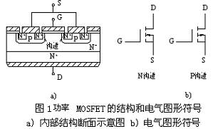
According to the difference of vertical conductive structure, it is divided into VVMOSFET which realizes vertical conduction by V-groove and VDMOSFET (Vertical Double-diffused MOSFET) which has vertical conductive double-diffused MOS structure. This paper mainly discusses VDMOS device as an example.
The power MOSFET is a multi-integrated structure. For example, International Rectifier's HEXFET uses a hexagonal unit; Siemens' SIP MOSFET uses a square unit; Motorola's TMOS uses a rectangular unit. "Glyph arrangement.
2.2 Working principle of power MOSFET
Cutoff: Positive power is applied between the drain and source, and the voltage between the gate and source is zero. The PN junction J1 formed between the P base region and the N drift region is reversely biased, and no current flows between the drain and the source.
Conductive: A positive voltage UGS is applied between the gate and source, and the gate is insulated, so no gate current flows. However, the positive voltage of the gate pushes the holes in the P region below it, and attracts the minority electrons in the P region to the surface of the P region below the gate.
When UGS is greater than UT (on voltage or threshold voltage), the electron concentration on the surface of the P region under the gate will exceed the hole concentration, so that the P-type semiconductor is inverted into an N-type and becomes an inversion layer, and the inversion layer forms an N-channel. The PN junction J1 disappears and the drain and source are conducting.
2.3 Basic characteristics of power MOSFET
2.3.1 Static characteristics; its transfer characteristics and output characteristics are shown in Figure 2.
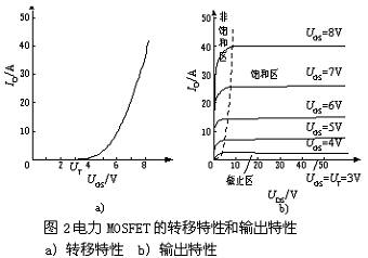
The relationship between the drain current ID and the gate-to-source voltage UGS is called the transfer characteristic of the MOSFET. When the ID is large, the relationship between ID and UGS is approximately linear, and the slope of the curve is defined as the transconductance Gfs.
The volt-ampere characteristics of the MOSFET (output characteristics): a cut-off region (corresponding to the GTR cut-off region); a saturation region (corresponding to the amplification region of the GTR); and an unsaturated region (corresponding to the saturation region of the GTR). The power MOSFET operates in a switching state, that is, switching back and forth between the cutoff region and the unsaturated region. There is a parasitic diode between the drain and source of the power MOSFET, and the device is turned on when a reverse voltage is applied between the drain and the source. The on-resistance of the power MOSFET has a positive temperature coefficient, which is advantageous for current sharing when the devices are connected in parallel.
2.3.2 Dynamic characteristics; the test circuit and the switching process waveform are shown in Figure 3.

Turn-on process; turn-on delay time td(on)—the time period between the time when the front edge is up to uGS=UT and the iD begins to appear;
Rise time tr—the period during which uGS rises from uT to the gate voltage UGSP where the MOSFET enters the unsaturated region;
The iD steady state value is determined by the drain supply voltage UE and the drain load resistance. The size of UGSP is related to the steady state value of iD. After UGS reaches UGSP, it continues to rise until it reaches steady state, but iD has not changed.
The turn-on time ton—the sum of the turn-on delay time and the rise time.
Shutdown delay time td(off)—upup drops to zero, Cin discharges through Rs and RG, and uGS begins to decrease to zero when exponentially decreasing to UGSP.
Fall time tf - uGS continues to fall from UGSP, iD decreases, to uGS
Turn-off time toff—the sum of the turn-off delay time and the fall time.
2.3.3 Switching speed of the MOSFET.
The switching speed of MOSFET has a great relationship with Cin charge and discharge. Users can't reduce Cin, but it can reduce the internal resistance Rs of the drive circuit to reduce the time constant and speed up the switching speed. The MOSFET is only conductive by many sub-substations, so there is no minority storage effect. The turn-off process is very fast, switching time is between 10 and 100 ns, and the operating frequency is above 100 kHz, which is the highest among the main power electronic devices.
The field control device requires almost no input current when it is static. However, in the switching process, the input capacitor needs to be charged and discharged, and a certain driving power is still required. The higher the switching frequency, the greater the drive power required.
2.4 Improvement of dynamic performance
In addition to considering the voltage, current, and frequency of the device, it must be known how to protect the device in the application without damaging the device in transient changes. Of course, the thyristor is a combination of two bipolar transistors, and the large capacitance due to the large area, so its dv/dt capability is relatively fragile. For di/dt, it also has an extension problem of the conduction area, so it also brings quite strict restrictions.
The situation of power MOSFETs is quite different. Its dv/dt and di/dt capabilities are often measured in terms of nanoseconds (rather than microseconds). But despite this, it also has dynamic performance limitations. These can be understood from the basic structure of the power MOSFET.
Figure 4 shows the structure of the power MOSFET and its corresponding equivalent circuit. In addition to the presence of capacitance in almost every part of the device, it must also be considered that the MOSFET is also connected in parallel with a diode. At the same time, from a certain point of view, it also has a parasitic transistor. (Like IGBTs also parasitize a thyristor). These aspects are important factors in studying the dynamic characteristics of MOSFETs.
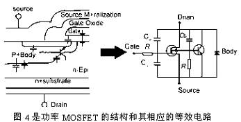
First, the intrinsic diode attached to the MOSFET structure has a certain avalanche capability. It is usually expressed by a single avalanche ability and repeated avalanche ability. When the reverse di/dt is large, the diode will withstand a very fast pulse spike, which may enter the avalanche zone and may damage the device once it exceeds its avalanche capability. As a PN junction diode, careful study of its dynamic characteristics is quite complicated. They are very different from the simple concept that we generally understand that blocking is reversed when the PN junction is positive. When the current drops rapidly, the diode loses its reverse blocking capability in one stage, the so-called reverse recovery time. When the PN junction is required to be turned on quickly, there will be a period of time that does not show a very low resistance. In the power MOSFET, once the diode is forward implanted, the injected minority carriers also increase the complexity of the MOSFET as a multi-sub-device.
During the design of the power MOSFET, measures are taken to make the parasitic transistors therein as ineffective as possible. The measures are different in different generations of power MOSFETs, but the general principle is to make the lateral resistance RB under the drain as small as possible. The parasitic bipolar thyristor begins to fail because only the lateral resistance under the drain N region flows through a sufficient current to establish a positive bias for this N region. However, under severe dynamic conditions, the lateral current due to dv/dt through the corresponding capacitance may be sufficiently large. At this point, the parasitic bipolar transistor will start, which may damage the MOSFET. Therefore, attention must be paid to the individual capacitors inside the power MOSFET device (which is the channel of dv/dt) when considering transient performance.
Transient conditions are closely related to the condition of the line, and this aspect should be given sufficient attention in the application. A thorough understanding of the device will help to understand and analyze the corresponding problem.
3. Principle and performance analysis of high voltage MOSFET
In power semiconductor devices, MOSFETs play an important role in various power conversions, especially high-frequency power conversion, with high speed, low switching loss, and low drive loss. In the low-voltage field, MOSFETs have no competitors, but as the withstand voltage of MOS increases, the on-resistance increases with a power of 2.4-2.6, and its growth rate has caused MOSFET makers and users to reduce by tens of times. Rated current, in contradiction between the rated current, on-resistance and cost. Even so, the on-resistance of the high-voltage MOSFET at the rated junction temperature is still high, and the MOSFET with a withstand voltage of 500V or higher has a high turn-on voltage at rated junction temperature and rated current, with a withstand voltage of 800V. The above turn-on voltage is astonishingly high, and the conduction loss accounts for 2/3-4/5 of the total loss of the MOSFET, which greatly limits the application.
3.1 Principle and method of reducing the on-resistance of high-voltage MOSFET
3.1.1 On-resistance distribution of MOSFETs with different withstand voltages.
For different withstand voltage MOSFETs, the proportional distribution of the resistance of each part of the on-resistance is also different. For a MOSFET with a withstand voltage of 30V, the epitaxial layer resistance is only 29% of the total on-resistance, and the epitaxial layer resistance of the MOSFET with a withstand voltage of 600V is 96.5% of the total on-resistance. From this, it can be inferred that the on-resistance of a MOSFET with a withstand voltage of 800V will be almost occupied by the epitaxial layer resistance. To achieve a high blocking voltage, a high resistivity epitaxial layer must be used and thickened. This is the root cause of the high on-resistance caused by conventional high voltage MOSFET structures.
3.1.2 Ideas for reducing the on-resistance of high-voltage MOSFETs.
Increasing the die area can reduce the on-resistance, but the cost of the increase is not allowed by commercial products. The introduction of minority carrier conduction can reduce the on-state voltage drop, but the cost is the reduction of the switching speed and the tail current, the switching loss increases, and the high speed of the MOSFET is lost.
The above two methods can not reduce the on-resistance of the high-voltage MOSFET. The remaining idea is how to solve the high doping and low resistivity of the low-doping, high-resistivity region and the conductive channel that block the high voltage. For example, a low-doped high-withstand voltage epitaxial layer, except for conduction, can only increase the on-resistance and has no other use. In this way, whether the conductive channel can be realized with high doping and lower resistivity, and when the MOSFET is turned off, try to make the channel pinch off in some way, so that the whole device withstand voltage depends only on the low-doped N-epitaxial. Floor. Based on this idea, INFINEON introduced the COOLMOS with a built-in transverse electric field with a withstand voltage of 600V in 1988, which made this idea possible. A schematic diagram of the cross-sectional structure of the high-voltage MOSFET with a built-in transverse electric field and a high blocking voltage and low on-resistance are shown in FIG. 5.
Unlike conventional MOSFET structures, a built-in lateral electric field MOSFET is embedded in the vertical P region sandwiching the N region of the vertical conductive region, so that when the MOSFET is turned off, a vertical electric field is established between the vertical P and N, and the vertical conductive region N The doping concentration is higher than the doping concentration of its epitaxial region N-.
When VGS<VTH, the N-type conductive channel generated by the inversion of the electric field cannot be formed, and a positive voltage is applied between D and S, so that the internal PN junction of the MOSFET is reversely biased to form a depletion layer, and the vertical conductive N region is formed. Exhausted. This depletion layer has a longitudinal high blocking voltage as shown in Fig. 5(b), at which time the withstand voltage of the device depends on the withstand voltage of P and N-. Therefore, low doping and high resistivity of N- are necessary.
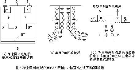
When CGS>VTH, an N-type conductive channel generated by an electric field inversion is formed. Electrons in the source region enter the depleted vertical N region and positive charges through the conductive channel, thereby restoring the depleted N-type characteristics, and thus the conductive channel is formed. Since the vertical N region has a lower resistivity, the on-resistance is significantly lower than that of a conventional MOSFET.
From the above analysis, it can be seen that the blocking voltage and the on-resistance are in different functional areas. Separating the blocking voltage from the on-resistance function solves the contradiction between the blocking voltage and the on-resistance, and also converts the surface PN junction at the time of blocking into a buried PN junction. At the same N-doping concentration, the resistance The breaking voltage can be further improved.
3.2 Main characteristics of built-in lateral electric field MOSFET
3.2.1 Reduction of on-resistance.
INFINEON's built-in lateral electric field MOSFETs withstand voltages of 600V and 800V have the same die area and on-resistance down to 1/5, 1/10 of conventional MOSFETs, respectively, compared to conventional MOSFETs; The on-resistance drops to 1/2 and about 1/3, respectively. Under the rated junction temperature and rated current, the turn-on voltage dropped from 12.6V, 19.1V to 6.07V, 7.5V, respectively; the conduction loss dropped to 1/2 and 1/3 of the conventional MOSFET. Due to the reduction of conduction loss, the heat is reduced and the device is relatively cool, so it is called COOLMOS.
3.2.2 Reduction of package and reduction of thermal resistance.
The COOLMOS die of the same current rating is reduced to 1/3 and 1/4 compared to conventional MOSFETs, reducing the package size by two packages.
Since the COOLMOS die thickness is only 1/3 of the conventional MOSFET, the TO-220 package RTHJC is reduced from the conventional 1 °C / W to 0.6 ° C / W; the rated power is increased from 125 W to 208 W, which improves the heat dissipation capability of the die.
.2.3 Improvements in switching characteristics.
The gate charge and switching parameters of COOLMOS are better than conventional MOSFETs. Obviously, due to the reduction of QG, especially QGD, the switching time of COOLMOS is about 1/2 of that of conventional MOSFETs; the switching loss is reduced by about 50%. The turn-off time is also related to the low internal gate resistance of COOLMOS (<1Ω=.
3.2.4 Avalanche breakdown resistance and SCSOA.
Currently, the new MOSFETs are invariably resistant to avalanche breakdown. COOLMOS is also resistant to avalanche. At the same rated current, the IAS of COOLMOS is the same as ID25°C. However, due to the reduction in die area, IAS is smaller than conventional MOSFETs, and with the same die area, both IAS and EAS are larger than conventional MOSFETs.
One of the biggest features of COOLMOS is that it has a short-circuit safe operating area (SCSOA), which is not available in conventional MOS. The acquisition of COSOMOS's SCSOA is mainly due to changes in transfer characteristics and reduced thermal resistance of the die. The transfer characteristics of COOLMOS are shown in Figure 6. It can be seen from Fig. 6 that when VGS>8V, the drain current of COOLMOS no longer increases and is in a constant current state. Especially when the junction temperature rises, the constant current value decreases. At the highest junction temperature, it is about twice the ID25°C, which is 3-3.5 times of the normal operating current. In the short-circuit state, the drain current does not rise to an unacceptable ten-fold ID25°C due to the 15V driving voltage of the gate, so that the power dissipated by the COOLMOS in the short-circuit is limited to 350V×2ID25°C, as much as possible. Reduces die heating when shorted. The reduced thermal resistance of the die allows the heat generated by the die to be quickly dissipated to the package, suppressing the rate of rise of the die temperature. Therefore, COOLMOS can be driven at a normal gate voltage and withstand a 10 ΜS short-circuit shock at a voltage of 0.6 VDSS. The time interval is greater than 1 S and 1000 times without damage, so that COOLMOS can be effectively protected like a IGBT in the event of a short circuit.

3.3 Development Status of High Voltage MOSFETs with Built-in Transverse Electric Fields
Following the introduction of COOLMOS in INFINEON in 1988, ST introduced the internal structure of 500V similar to COOLMOS in early 2000, so that 500V, 12A MOSFET can be packaged in TO-220 package, with on-resistance of 0.35Ω, 0.4Ω lower than IRFP450, current The rating is similar to the IRFP450. IXYS also has MOSFETs using COOLMOS technology. IR also introduced SUPPER220, a super MOSFET in the SUPPER247 package, rated at 35A, 59A, with on-resistance of 0.082Ω and 0.045Ω respectively, and a conduction voltage drop of approximately 4.7V at 150°C. From the comprehensive indicators, these MOSFETs are superior to conventional MOSFETs, not because the on-resistance decreases proportionally with the increase of the die area. Therefore, it can be considered that the above MOSFET must have a special structure similar to the transverse electric field. Attempts to reduce the turn-on voltage drop of high-voltage MOSFETs has become a reality and will certainly drive the application of high-voltage MOSFETs.
3.4 Comparison of COOLMOS and IGBT
The high-temperature turn-on voltage drop of 600V, 800V withstand voltage COOLMOS is about 6V, 7.5V, the turn-off loss is reduced by 1/2, and the total loss is reduced by 1/2 or more, so that the total loss is 40%-50% of the conventional MOSFET. Conventional 600V withstand voltage MOSFET conduction loss accounts for about 75% of the total loss, corresponding to the same total loss ultra-high speed IGBT balance point of 160KHZ, of which switching loss accounts for about 75%. Since the total loss of COOLMOS drops to 40%-50% of the conventional MOSFET, the corresponding IGBT loss balance frequency will be reduced from 160KHZ to about 40KHZ, which increases the application of MOSFET in high voltage.
As can be seen from the above discussion, the new high-voltage MOSFET solves the problem of high on-voltage drop caused by long-term high-voltage MOSFETs; it can simplify the design of the whole machine, such as the volume of the heat sink can be reduced to about 40%; the drive circuit and the snubber circuit are simplified; Anti-avalanche breakdown capability and short-circuit resistance; simplify the protection circuit and improve the reliability of the whole machine.
4. Power MOSFET drive circuit
The power MOSFET is a voltage type driving device, which has no storage effect of minority carriers, and has high input impedance, so the switching speed can be high, the driving power is small, and the circuit is simple. However, the inter-electrode capacitance of the power MOSFET is large, and the relationship between the input capacitance CISS, the output capacitance COSS, and the feedback capacitance CRSS and the interelectrode capacitance can be expressed as:
The gate input of the power MOSFET is equivalent to a capacitive network whose operating speed is related to the internal impedance of the drive source. Due to the presence of CISS, the gate drive current is almost zero during static, but a certain drive current is still required during the turn-on and turn-off dynamics. Assuming that the gate voltage value required for saturation switching of the switching transistor is VGS, the turn-on time TON of the switching transistor includes two parts of the turn-on delay time TD and the rise time TR.
During the switch-off process, CISS discharges through ROFF, COSS is charged by RL, COSS is larger, VDS(T) rises slowly, and as VDS(T) rises slowly, COSS increases rapidly with VDS(T) When reduced to near zero, VDS(T) rises again rapidly.
According to the above analysis of the characteristics of the power MOSFET, the driving usually requires that the trigger pulse have a fast rising and falling speed; 2 when charging, the low-resistance gate capacitance is charged, and when the power is turned off, the gate is provided with a low-resistance discharging circuit. In order to improve the switching speed of the power MOSFET; 3 in order to make the power MOSFET reliably trigger conduction, the trigger pulse voltage should be higher than the turn-on voltage of the tube, in order to prevent mis-conduction, a negative gate-source voltage should be provided when it is turned off; 4 power switch tube The driving current required for switching is the charging and discharging current of the gate capacitor. The larger the capacitance between the power transistors, the larger the required current, that is, the greater the load carrying capacity.
4.1 Introduction and Analysis of Several MOSFET Drive Circuits
4.1.1 Non-isolated complementary drive circuit.
Figure 7 (a) shows a common low-power drive circuit that is simple, reliable, and low in cost. Suitable for small power switching devices that do not require isolation. The driving circuit shown in Figure 7(b) has a fast switching speed and strong driving capability. In order to prevent the two MOSFETs from being through, a small 0.5~1Ω resistor is usually connected in series for current limiting. The circuit is suitable for medium power that does not require isolation. Switching device. These two circuits are characterized by a simple structure.
The power MOSFET is a voltage type control device that is turned on as long as the voltage applied between the gate and the source exceeds its threshold voltage. Due to the junction capacitance of the MOSFET, a sudden rise in voltage across the drain and source when turned off will cause an interference voltage across the gate and source through the junction capacitance. The commonly used complementary drive circuit has a small off-circuit impedance and a fast turn-off speed, but it does not provide a negative voltage, so the anti-interference is poor. In order to improve the anti-interference of the circuit, a circuit with a composition of V1, V2, R can be added on the basis of the driving circuit to generate a negative voltage, and the circuit schematic is shown in FIG.
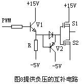
When V1 is turned on, V2 is turned off, the gate and source of the upper tube of the two MOSFETs are discharged, and the gate and source of the lower tube are charged, that is, the upper tube is turned off, and the lower tube is turned on, then the driven power tube is driven. When V1 is turned off, V2 is turned on, the upper tube is turned on, and the lower tube is turned off, so that the driven tube is turned on. Because the gate and source of the upper and lower tubes are charged and discharged through different circuits, the circuit containing V2, because V2 will continuously exit saturation until it is turned off, the conduction is slower than S1 for S1. The conduction is faster than the shutdown, so the degree of heat generation of the two tubes is not exactly the same, and S1 is more severe than S2.
The disadvantage of this driving circuit is that it requires dual power supply, and since the value of R cannot be too large, V1 will be deeply saturated and affect the shutdown speed, so there will be a certain loss on R.
4.1.2 Isolated Drive Circuit
(1) Forward drive circuit. The circuit principle is shown in Figure 9(a), N3 is the demagnetization winding, and S2 is the driven power tube. R2 is a damping resistor that prevents the power tube gate and source terminal voltage from oscillating. Since the leakage inductance is not required to be small, and from the viewpoint of speed, R2 is generally small, so it is ignored in the analysis.

The equivalent circuit diagram is shown in Figure 9(b). The secondary side of the pulse is not required to be connected in parallel with a resistor R1. It acts as a dummy load of the forward converter to eliminate the false oscillation of the output voltage during the turn-off. It can also be used as an energy bleeder circuit when the power MOSFET is turned off. The conduction speed of the driving circuit is mainly related to the size of the driven S2 gate, the source equivalent input capacitance, the speed of the driving signal of S1, and the magnitude of the current that S1 can provide. It can be seen from simulation and analysis that the smaller the duty ratio D is, the larger R1 is, the larger L is, and the smaller the magnetizing current is, the smaller the U1 value is, and the slower the shutdown speed is. This circuit has the following advantages:
1 The circuit structure is simple and reliable, and the isolation drive is realized.
2 Only a single power supply can provide positive and negative voltages during turn-on.
When the duty ratio is fixed, the drive circuit also has a faster switching speed through reasonable parameter design.
The shortcomings of this circuit are as follows: First, since the secondary side of the isolation transformer needs anti-oscillation due to the false load, the circuit loss is large; the second is that the shutdown speed changes greatly when the duty ratio changes. When the pulse width is narrow, the turn-off speed of the MOSFET gate is slowed due to the reduced energy stored.
(2) A complementary drive circuit with an isolation transformer. As shown in FIG. 10, V1 and V2 are complementary operations, capacitor C functions to isolate DC, and T1 is a high frequency, high magnetic flux magnetic ring or magnetic can.

When the conduction is on, the voltage on the isolation transformer is (1-D)Ui, and when it is off, it is D Ui. If the main power tube S is reliably turned on, the voltage is 12V, and the isolation transformer's original secondary side ratio is N/N2 is 12/[ (1-D)Ui]. In order to ensure that the GS voltage is stable during the on-time, the C value can be slightly larger. This circuit has the following advantages:
1 The circuit structure is simple and reliable, and has electrical isolation. When the pulse width changes, the drive's turn-off capability does not change.
2 This circuit requires only one power supply, that is, it operates as a single power supply. The function of the DC blocking capacitor C can provide a negative pressure when the driven tube is turned off, thereby accelerating the shutdown of the power tube and having high anti-interference ability.
However, one of the major drawbacks of this circuit is that the magnitude of the output voltage will vary with the duty cycle. When D is small, the negative voltage is small, the anti-interference of the circuit is deteriorated, and the forward voltage is high. It should be noted that the amplitude does not exceed the allowable voltage of the MOSFET gate. When D is greater than 0.5, the driving voltage forward voltage is less than its negative voltage. At this time, it should be noted that the negative voltage value does not exceed the MOAFET gate allowable voltage. Therefore, the circuit is suitable for applications where the duty cycle is fixed or the duty cycle varies little and the duty cycle is less than 0.5.
(3) Drive circuit composed of integrated chip UC3724/3725
The circuit configuration is as shown in FIG. The UC3724 is used to generate a high frequency carrier signal, and the carrier frequency is determined by the capacitance CT and the resistance RT. Generally, the carrier frequency is less than 600 kHz, and high-frequency modulated waves are generated at both ends of the 4 and 6 legs. After being separated by the high-frequency small-magnetic ring transformer, the signals are sent to the UC3725 chip 7 and 8 and modulated by the UC3725 to obtain the driving signal. The UC3725 has a shaw inside. The special-purpose rectifier bridge rectifies the high-frequency modulated waves of pins 7 and 8 into a DC voltage for driving. Generally speaking, the higher the carrier frequency, the smaller the driving delay, but the higher the anti-interference is. The larger the magnetizing inductance of the isolation transformer is, the smaller the magnetizing current is. The less the UC3724 generates less heat, but the larger the number of turns, the larger the number of turns causes the parasitic parameters to become larger. It also reduces the anti-interference ability. According to the experimental data, it is concluded that the signal with a switching frequency less than 100 kHz generally takes a carrier frequency of (400-500) kHz, and the transformer uses a high-frequency toroidal core such as 5K, 7K, etc., and the primary side magnetization inductance is less than about 1 milliheng is good. This kind of driving circuit is only suitable for the case where the signal frequency is less than 100 kHz. If the signal frequency is too high relative to the carrier frequency, the relative delay is too much, and the required driving power is increased. The heating temperature rise of the UC3724 and UC3725 chips is higher, so 100 kHz. The above switching frequency is only available for MOSFETs with smaller pole capacitance. It is a good driving circuit for a switching frequency of less than 100 kHz around 1 kVA. The circuit has the following characteristics: single power supply operation, control signal and drive isolation, simple structure and small size, especially suitable for occasions where the duty cycle changes are uncertain or the signal frequency also changes.

Hydrogel Screen Protector Sheets
Universal Screen Protector, TPU Screen Protector, Hydrogel Protective Film, Mobile Phone Screen Protector, Hydrogel Screen Protector, TPU Protective Film
Shenzhen Jianjiantong Technology Co., Ltd. , https://www.jjttpucuttingplotter.com