1. Frequency-division multiplier: The DCM can perform MulTIply or Divide on the input clock to obtain a new output clock.
2. Go to Skew: DCM can also eliminate the Skew of the Clock. The so-called Skew is the delay difference of the same clock arriving at different locations due to transmission.
3. Phase shift: The DCM can also achieve phase shift output to the input clock. This phase shift is generally a fraction of the clock cycle.
4. Global clock: The DCM and the internal global clock distribution network of the FPGA are tightly coupled, so the performance is excellent.
5. Level conversion: With DCM, different standard clocks can be output.
DCM features and capabilities (Spartan-3 series as an example)
Quantity: 4 DCM/FPGA (with exceptions)
-- Should be enough
Digital Frequency Synthesizer Input (CLKIN): 1-280MHz
Delayed phase-locked loop input (CLKIN): 18-280 MHz
Clock input source (CLKIN):
Global Buffer Input Pad
Global Buffer Output
General-Purpose I/O (No Deskew)
Internal Logic (No Deskew)
-- The last two are the external ordinary IO port and the internal logic, there is no Deskew, so the clock quality will not be very good.
Frequency synthesizer output (CLKFX, CLKFX180): M/D times CLKIN, where
M=2..32
D=1..32
-- It seems that the maximum frequency can be multiplied by 32 times and the minimum by 16 frequency.
Clock Dividor Output (CLKDV): is the following division of CLKIN
1.5, 2, 2.5, 3, 3.5, 4, 4.5, 5, 5.5, 6, 6.5, 7, 7.5, 8, 9, 10, 11, 12, 13, 15, Or 16
-- No discovery, the maximum frequency is 16. However, it is possible to support half frequency division rather than using a frequency synthesizer.
Frequency multiplier output (CLK2X, CLK2X180): 2 times the frequency of CLKIN
Clock CondiTIoning, Duty Cycle Adjustment: This applies to all clock outputs with a duty cycle of 50%.
1/4-cycle phase-shift output (CLK0/90/180/270): This is a 1/4-cycle phase-shift output from CLKIN.
Half-cycle phase shift output (CLK0/180, CLK2X/180, CLKFX/180): Paired clock output with a phase difference of 180 degrees.
Phase shift accuracy: The highest precision is 1/256 of the clock period.
Clock output: 9
Clock output to the global clock network: up to 4 out of 9
Interconnection to the General Purpose: Up to 9
To output feet: up to 9
-- It can be seen that 9 clock outputs can freely link internal signals or external outputs, but there are only 4 paths to the global clock network.
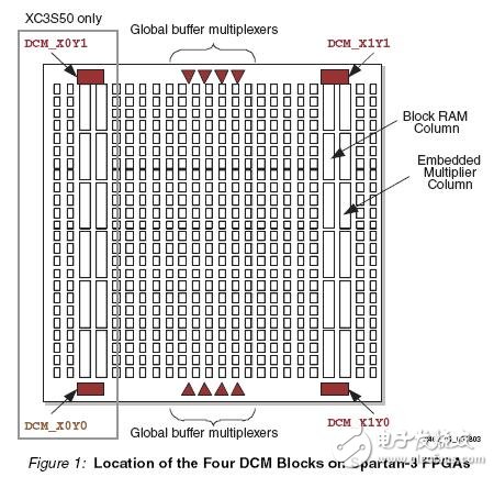
Where is DCM's position?Let's take the Spartan3 series as an example.
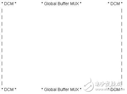
The FPGA looks like a square. The most edge is the IO Pad. Remove the IO Pad and the inside is still a square. There is a DCM on each of the four corners. In the middle of the upper edge and the lower edge, there is a global buffer MUX. The advantage of this is that the output of the four DCMs can be directly connected to the entrance of the global Buffer.
The following is a hand-drawn sketch, it is ugly right, huh, huh.
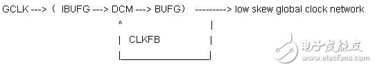
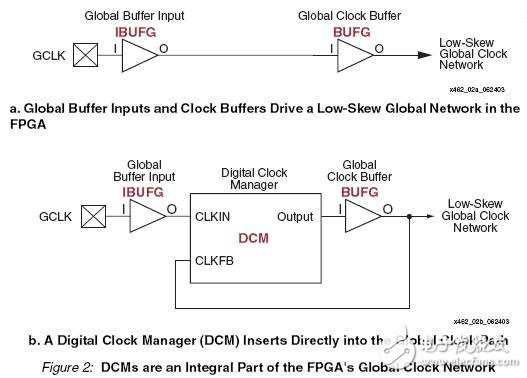
DCM is an optional part of the global clock network
In general, the clock enters the global clock network through a "global input buffer" and "global clock buffer". As follows
GCLK ---》( IBUFG ---) BUFG ---》 Low Skew Global Clock Network
When needed, DCM also becomes a part of the global clock network.
DLL delay locked loop
It is a delay locked loop, but I think the delay compensation loop is more appropriate. Because the main function of the DLL is to eliminate the delay between the input clock and the output clock, the input and output appear to be transparent connections externally.
The principle for implementing this function is that the DLL observes the actual line delay through the output clock CLK0 or CLK2X and then compensates internally.
In a word, the core function of a DLL is no delay.
The outputs of the DLL are CLK0, CLK90, CLK180, CLK270, CLK2X, CLK2X180, and CLKDV.
2. DFS digital frequency synthesis
The main function of DFS is to synthesize new frequencies using CLKIN.
The synthesized parameters are: M(MulTIplier) and D(Divisor). Through the combination of MD to achieve a variety of frequency and frequency division.
If you do not use a DLL, the synthesis frequency of DFS and CLKIN have no phase relationship, because without delay compensation, the phases are not synchronized.
3. PS phase shift
Note that this phase offset is not used in the DLL output CLK90/180/270. This PS can shift the phase of all 9 output signals of the DCM. The unit of offset is a fraction of CLKIN.
Dynamic offset adjustment can also be performed during operation. The unit of adjustment is 1/256 of the clock.
This function is not commonly used by us.
4. State logic
This part consists of the LOCKED signal and STATUS[2:0]. The LOCKED signal indicates whether the output is synchronized (in phase) with CLKIN. STATUS then indicates the status of the DLL and the PS.
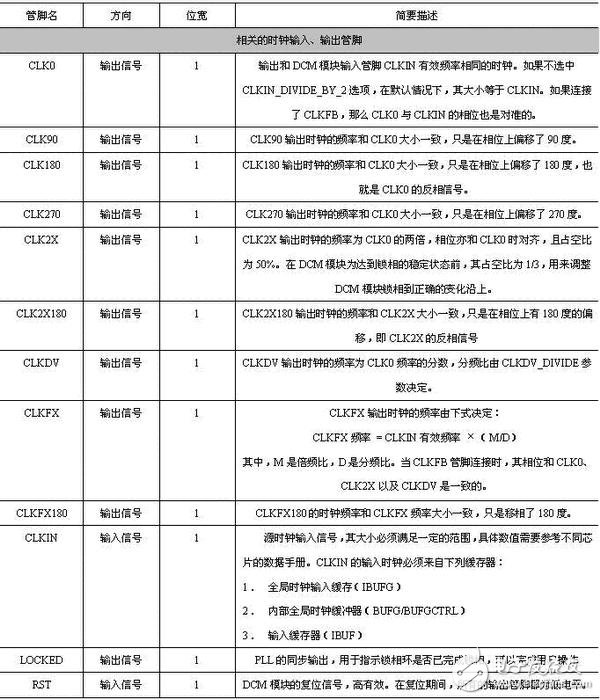
DCM_BASEDCM_BASE is an abbreviation of the basic digital clock management module. It is a phase- and frequency-configurable digital phase-locked loop (PLL) circuit and is often used for complex clock management in an FPGA system. If frequency and phase dynamic reconfiguration are required, the DCM_ADV primitive can be used; if phase dynamic offset is required, the DCM_PS primitive can be used. The RTL structure of the DCM series primitives is shown in Figure 3-8.
The module interface signals are described in Table 3-8.
The DCM_BASE component can be generated by Xilinx's IP Wizard wizard or directly through the following instantiation code. Its Verilog's instantiation code template is:
// DCM_BASE: Base Digital Clock Manager Circuit
// Applicable chip: Virtex-4/5
// Xilinx HDL Library Wizard version, ISE 9.1
DCM_BASE # (
.CLKDV_DIVIDE(2.0),
// The CLKDV divider ratio can be set to: 1.5,2.0,2.5,3.0,3.5,4.0,4.5,5.0,5.5,6.0,6.5
// 7.0,7.5,8.0,9.0,10.0,11.0,12.0,13.0,14.0,15.0 Or 16.0
.CLKFX_DIVIDE(1), // Can Be Any Integer From 1 To 32
// Divider ratio of CLKFX signal, any integer between 1 and 32
.CLKFX_MULTIPLY(4),
// The multiplier of the CLKFX signal, which can be any integer between 2 and 32
.CLKIN_DIVIDE_BY_2 ("FALSE"),
// Input signal divided by 2 enable signal, can be set to TRUE/FALSE
.CLKIN_PERIOD(10.0),
// Specify the period of the input clock in Ns. The value range is 1.25~1000.00.
.CLKOUT_PHASE_SHIFT("NONE"),
// Specifies the phase shift mode, which can be set to NONE or FIXED
.CLK_FEEDBACK("1X"),
// Specify the frequency of the feedback clock, which can be set to NONE, 1X, or 2X. The corresponding frequency relationship is for CLK0.
.DCM_PERFORMANCE_MODE("MAX_SPEED"),
// DCM module performance mode, set to MAX_SPEED or MAX_RANGE
.DESKEW_ADJUST("SYSTEM_SYNCHRONOUS"),
// Jitter adjustment, can be set to source synchronization, system synchronization, or any integer between 0 and 15
.DFS_FREQUENCY_MODE("LOW"),
// Digital frequency synthesis mode, can be set to LOW or HIGH
.DLL_FREQUENCY_MODE("LOW"),
// DLL's frequency mode can be set to LOW, HIGH, or HIGH_SER
.DUTY_CYCLE_CORRECTION("TRUE"),
// Set whether to use double-cycle correction, set to TRUE or FALSE
.FACTORY_JF(16''Hf0f0),
// 16-bit JF factor parameters
.PHASE_SHIFT(0),
// The value of the fixed phase shift, which can be set to any integer between -255 and 1023
.STARTUP_WAIT("FALSE")
// Delay the configuration of the DONE pin after the DCM phase lock, which can be set to TRUE/FALSE
) DCM_BASE_inst (
.CLK0 (CLK0), // 0 degree phase-shifted DCM clock output
.CLK180 (CLK180), // 180 degree phase-shifted DCM clock output
.CLK270(CLK270), // 270-degree phase-shifted DCM clock output
.CLK2X(CLK2X), // 2 times output of DCM module
.CLK2X180(CLK2X180), // Double frequency output of DCM module with 180 degree phase shift
.CLK90(CLK90), // 90 degree phase-shifted DCM clock output
.CLKDV(CLKDV), // Divider output of DCM module, divide ratio is CLKDV_DIVIDE
.CLKFX(CLKFX), // DCM Synthesis Clock Output, Divider Ratio (M/D)
.CLKFX180 (CLKFX180), // 180-degree phase-shifted DCM synthesis clock output
.LOCKED(LOCKED), // DCM lock status output signal
.CLKFB(CLKFB), // Feedback clock signal for DCM module
.CLKIN(CLKIN), // Clock input signal for DCM module
.RST(RST) // Asynchronous reset signal of DCM module
);
// End the instantiation process of the DCM_BASE module
When analyzing the synthesis results, the RTL structure of DCM series primitives is shown in Figure 3-36.
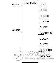
Figure 3-36 RTL level structure of DCM module
Spartan-3 DCM CompatibilityS3's DCM and Virtex-II and Pro's DCM functions are basically the same. However, the technology of the S3 DCM belongs to the 3rd generation technology, and therefore there is further improvement in the anti-noise performance and phase shift capability. (Objectively speaking, it is not particularly important for our general application.)
However, compared with the Spartan-2 series, there has been a great improvement. S2 series does not call DCM to call DLL. It can be seen that functions such as DFS and PS are completely new. Therefore, S2 series has almost no multiplier and frequency division ability except for double frequency. From this point of view, S3 is really cool to use.
DCM input clock limit
As with all physical devices, the DCM's operating range is also limited. Since the requirements of DLL and DFS vary, the DCM input frequency limit also depends on whether DLL and DFS are used at the same time or whether they are used individually. If used at the same time, take the stricter limit as the limitation of the entire DCM system. Let's look at the independent restrictions of both.
Oh, this part of the content does not need to remember Oh, when you need to check the software or manual on it. As long as you understand that "the input frequency of CLKIN is limited, and DLL and DFS are used strictly when they are used at the same time", these principles are all right.
In addition to the clock restrictions, there are also certain limitations on the quality of the clock. There are three main reasons:
1. CLKIN Cycle-To-Cycle Jitter: Constrain the difference between the two CLKIN cycles before and after;
2. CLKIN Period Jitter: Constrains the difference between the maximum period and the minimum period in 1 million cycles;
3. CLKFB Path Delay Variation: Constrains the delay fluctuations of the feedback loop coming from the outside. This delay fluctuation is conceptually similar to Jitter.
Please check the manual for specific values ​​and know that there is such a thing.
How the LOCKED signal behavesThe LOCKED signal is used to indicate that the entire DCM system has been synchronized with CLKIN. Since the LOCKED signal is valid, the output clock can be used. Before that, the output clock may be in various complicated unstable states. Let's take a look at the behavioral state machine of the LOCKED signal.
FPGA configuration:
If (CLKIN has stabilized) Next_state = Judge synchronization;
Else Next_state = RST_DCM;
Determine synchronization:
If (already synchronized) Next_state = Judge synchronization;
Else Next_state = Synchronization failed;
Synchronization failure: Next_state = RST_DCM;
RST_DCM: Next_state = FPGA configuration;
Now take a look at the output in each state.
Case (State)
FPGA configuration: LOCKED = 0;
Judge synchronization: LOCKED = 1;
Synchronization failed: LOCKED = 0;
RST_DCM:LOCKED = 0;
Endcase
RST signal - restart lock
The RST signal is used to reset the relevant function of the DCM when the clock is unstable or loses lock, thus restarting lock tracking.
As an input signal, RST cannot be set by DCM itself, so we need our application design to control this RST signal, otherwise we need to ground it.
Setting RST will delay the position of Tap to 0, so Glitch or Duty Cycle may be changed and the phase offset will be reset back to the default value.
DCM Generation WizardWith ISE installed, you get a series of Accessories. With the Architecture Wizard, we can generate DCM modules. The generated DCM will produce 3 kinds of output:
1. A logical synthesis file instantiating a DCM (VHDL/Verilog in a manufacturer-specific format)
2. A UCF file controls a specific implementation
3. All other user settings are saved to the XAW (Xilinx Architecture Wizard) file.
Next describe the wizard usage steps.
1. Start the interface from ISE or Arch Wizard;
2. The first page to do the basic configuration: path, XAW file name, VHDL / Verilog selection, synthesis tool, FPGA model;
3. In the General Setup, you can see at a glance, do not elaborate, pay attention to the following points:
- CLKIN Source If you select External, CLKIN of the DCM is automatically connected to the IBUFG.
- Feedback If you select Internal, the feedback is from BUFG.
4. Advanced settings
- Select whether the configuration of the FPGA contains the lock of the DCM. If yes, the configuration completion signal DONE will be valid after the LOCKED signal is valid.
- Select whether CLKIN divides by two. Since the input frequency of the DCM is limited, it is made available by dividing by 2 for an input clock that is too high.
- Deskew adjustment. This option is recommended after consultation with Xilinx engineers.
5. Clock Output Buffer Setting
- By default, all outputs are linked to the BUFG global clock network entry
- Since the entrance of the global clock network is limited, users can customize the clock output port to connect to other types of Buffer
- Global Buffer: Buffer to enter the global clock network, a total of four, referred to as BUFG
- Enabled Buffer: It is still the above 4 global clock Buffer, but is configured to have enable signal control, referred to as BUFGCE
- Clock MUX: The above four global clock buffers, but configured as 2-To-1 MUX type selected by the S signal control, referred to as BUFGMUX
- Low Skew Line: No Buffer, only Skew
- Local Routing: connected to the local, Skew's requirements are not very strict
- None: disable output
- For the Enabled Buffer type and Clock Mux type, you need to specify the name of the En port
- Need to specify a name for the output clock signal or use the default
6. Set up DFS
- Set the target output frequency and press Calculate to automatically generate the M/D value and the jitter value
- Or manually set the M/D value and then press Calculate to automatically generate frequency and jitter values
7. Finally output the required 3 kinds of files.
Garden Equipment,Garden Pond Water Pump,Low Voltage Pond Pumps,Swimming Pool Pump
Sensen Group Co., Ltd.  , https://www.sunsunglobal.com