This year, the world is expected to sell more than 450 million mobile phones, 35 million laptops and 12 million personal digital assistants (PDAs) . These products are identical in two ways: first, they are all powered by batteries; second, they all have some form of noise-sensitive RF circuitry ( or additional circuitry ) . Obviously, mobile phones always use sensitive RF transceiver circuits, but adding such circuits to PDAs and handheld computers is still a recent development, and this is partly the result of the development of Bluetooth technology. At the same time, switching power supplies are gradually replacing linear regulators to extend battery life. The presence of both a noise source ( switching power supply ) and a noise-sensitive circuit in the product can cause interference problems.
The traditional solution is to keep the noise source circuit away from noise sensitive circuits. However, in today's handheld products, the design is very compact, so this method is no longer feasible , and solving the problem by adding shielding is not feasible in both cost and volume. The noise energy of traditional switching power supplies is mainly expressed in the form of concentrated narrow-band harmonics. However, if one of these harmonics happens to coincide with or is very close to a sensitive frequency ( such as the IF passband of the receiver ) , it is likely Cause interference.
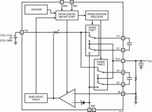
Figure 1 Â Simplified block diagram of non-inductive spread spectrum DC/DC converter
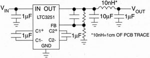
Figure 2 Â LTC3251 Buck Converter
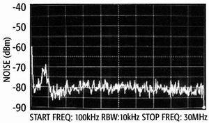
Figure 3 Â When using 10mF output capacitance (IO = 500mA) of the output noise spectrum LTC3251
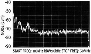
Figure 4 Â When the input noise spectrum using 1mF input capacitance (IO = 500mA) LTC3251 of
DC / DC (DC / DC) converter system clock is a dither technique was successfully employed. This method uses a pseudo-random sequence (PRN) to modulate the switching frequency by spread spectrum techniques to eliminate narrowband harmonics. Essentially, this approach "scatters" the noise over the entire frequency range and no longer concentrates on specific harmonics. Because the peak amplitude of the spread spectrum noise is much lower, the interference is greatly reduced. In the past, this technology was implemented in the form of discrete devices, but now with the advancement of the process, spread spectrum technology is integrated in newer DC/DC converter devices, which can save space.
Monolithic IC low noise solution supporting spread spectrum operation
To understand how to implement spread spectrum operation on-chip, let us take the block diagram shown in Figure 1 as an example. The two-phase switched capacitor charge pump of Figure 1 is used to step down the input voltage to obtain a stable output voltage. An external resistor divider is used to sense the output voltage while the error signal is used to modulate the charge pump output current to achieve regulation. The two charge pumps are excited by a two-phase non-overlapping clock. The two charge pumps work in parallel but are opposite in phase to each other. In the first phase of the clock, the current from VIN passes through the switch of charge pump 1 , and the external floating capacitor 1 reaches VOUT . During the first phase of the clock, the floating capacitor is also charged while the current is being transferred to VOUT . During the second phase of the clock, the floating capacitor 1 is connected to ground by VOUT , and the charge stored during the first phase of the clock is supplied to VOUT through the switch of the charge pump 1 . The charge pump 2 operates in the same manner, but the phase is opposite to that of the charge pump 1 . This two-phase structure greatly reduces output and input noise by continuously transferring charge from VIN to VOUT .
With this switching method, only half of the output current comes directly from VIN , which is 50% more efficient than traditional low-dropout (LDO) regulators . The spread spectrum operation is implemented by modulating the oscillator frequency on a per clock cycle basis based on changes in the pseudo-random number. Only a few percent modulation of the oscillator operating frequency can significantly reduce peak and harmonic noise.
Linear Technology's LTC3251 is one of the ICs that integrate on-chip spread spectrum . The LTC3251 is a high efficiency, low noise, non-inductive step-down DC/DC converter with an output current of 500mA . The spread-spectrum oscillator in the LTC3251 is designed such that the clock width of each cycle varies randomly, and the frequency range is limited to between 1 and 1.6 MHz . This has the advantage of spreading the switching noise over a wide frequency range. Figure 2 shows a typical application circuit for the LTC3251 . Figure 3 and Figure 4 show the output and input noise spectrum of the LTC3251 in Figure 2 at VIN = 3.6V , VOUT = 1.5V, and IOUT = 500mA , respectively. Due to the spread spectrum technology, the peak output noise can be significantly reduced (20dBm) with only half the capacity of the original output capacitor , and the input harmonics are almost eliminated with only one-tenth the capacity of the original input capacitor. Spread spectrum technology is dedicated to "continuous" mode and Burst Mode when the output current is greater than 50mA .
To meet the demands of handheld applications for power, wireless portability and reasonable battery life, designers have to integrate high-efficiency switching power supplies with noise-sensitive RF circuits. Traditional switching power supply architectures extend battery life, but may require costly and space-consuming filtering or shielding techniques. However, power ICs with "built-in" spread-spectrum switching are now available . With such ICs , harmonic interference to sensitive RF circuits can be mitigated even without traditional methods. Moreover, these small, relatively high output current and low noise power ICs are ideal for space-constrained, battery-powered applications.